SLAC’s high-speed electron camera uncovers a new ‘light-twisting’ behavior in an ultrathin material
Using SLAC’s instrument for ultrafast electron diffraction (MeV-UED), one of the lab’s world-leading tools for ultrafast science, researchers discovered how an ultrathin material can circularly polarize light. This discovery sets up a promising approach to manipulate light for applications in optoelectronic devices.
By Carol Tseng
While taking snapshots with the high-speed “electron camera” at the Department of Energy’s SLAC National Acceleratory Laboratory, researchers discovered new behavior in an ultrathin material that offers a promising approach to manipulating light that will be useful for devices that detect, control or emit light, collectively known as optoelectronic devices, and investigating how light is polarized within a material. Optoelectronic devices are used in many technologies that touch our daily lives, including light-emitting diodes (LEDs), optical fibers and medical imaging.
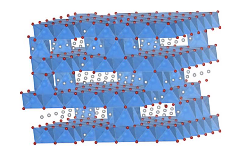
As reported in Nano Letters, the team, led by SLAC and Stanford professor Aaron Lindenberg, found that when oriented in a specific direction and subjected to linear terahertz radiation, an ultrathin film of tungsten ditelluride, which has desirable properties for polarizing light used in optical devices, circularly polarizes the incoming light.

SLAC researchers pioneer new methods in ultrafast science for sharper molecular movies
SLAC’s “electron camera” can reveal some of nature’s ultrafast processes. Now, researchers across the lab have collaborated to achieve improvements to that tool to make its molecular movies even sharper, keeping SLAC at the forefront of pioneering tools for ultrafast science.
Terahertz radiation lies between the microwave and the infrared regions in the electromagnetic spectrum and enables novel ways of both characterizing and controlling the properties of materials. Scientists would like to figure out a way to harness that light for the development of future optoelectronic devices.
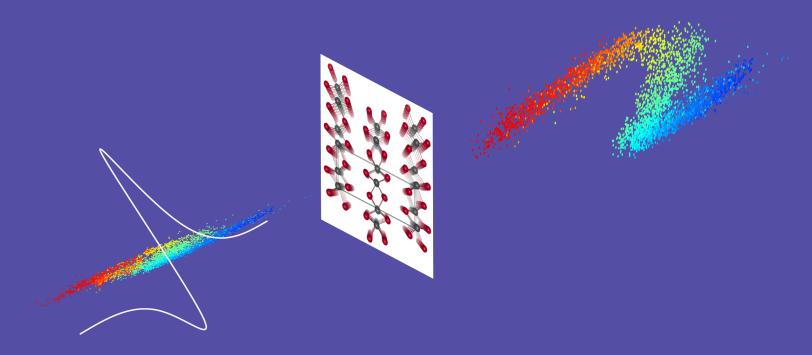
Capturing a material’s behavior under terahertz light requires an advanced instrument capable of recording the interactions at ultrafast speeds, and SLAC’s world-leading instrument for ultrafast electron diffraction (MeV-UED) at the Linac Coherent Light Source (LCLS) can do just that. Whereas the MeV-UED is normally used to visualize the motion of atoms by measuring how they scatter electrons after hitting a sample with an electron beam, this new work used the femtosecond electron pulses to visualize the electric and magnetic fields of the incoming terahertz pulses, which caused the electrons to wiggle back and forth. In the study, circular polarization was indicated by images of the electrons that showed a circular pattern rather than a straight line.
The ultrathin material was a mere 50 nanometers thick. “This is 1,000 to 10,000 times thinner than what we typically need to induce this type of response,” said Lindenberg.
Researchers are excited about using these ultrathin materials, known as two-dimensional (2D) materials, to make optoelectronic devices smaller and capable of more functions. They envision creating devices from layers of 2D structures, like stacking Legos, Lindenberg said. Each 2D structure would be composed of a different material, precisely aligned to generate a specific type of optical response. These different structures and functionalities can be combined into compact devices that could find potential applications – for example, in medical imaging or other types of optoelectronic devices.
“This work represents another element in our toolbox for manipulating terahertz light fields, which in turn could allow for new ways to control materials and devices in interesting ways,” said Lindenberg.
The study was supported by the DOE Office of Science and used resources of the National Energy Research Scientific Computing Center (NERSC). LCLS and NERSC are DOE Office of Science user facilities.
Citation: E. Sie et al., Nano Letters, 8 May 2024 (https://doi.org/10.1021/acs.nanolett.4c00758)
For questions or comments, contact SLAC Strategic Communications & External Affairs at communications@slac.stanford.edu.
About SLAC
SLAC National Accelerator Laboratory explores how the universe works at the biggest, smallest and fastest scales and invents powerful tools used by researchers around the globe. As world leaders in ultrafast science and bold explorers of the physics of the universe, we forge new ground in understanding our origins and building a healthier and more sustainable future. Our discovery and innovation help develop new materials and chemical processes and open unprecedented views of the cosmos and life’s most delicate machinery. Building on more than 60 years of visionary research, we help shape the future by advancing areas such as quantum technology, scientific computing and the development of next-generation accelerators.
SLAC is operated by Stanford University for the U.S. Department of Energy’s Office of Science. The Office of Science is the single largest supporter of basic research in the physical sciences in the United States and is working to address some of the most pressing challenges of our time.