SLAC’s X-ray Laser Glimpses How Electrons Dance with Atomic Nuclei in Materials
Understanding how a material’s electrons interact with vibrations of its nuclear lattice could help design and control novel materials, from solar cells to high-temperature superconductors.
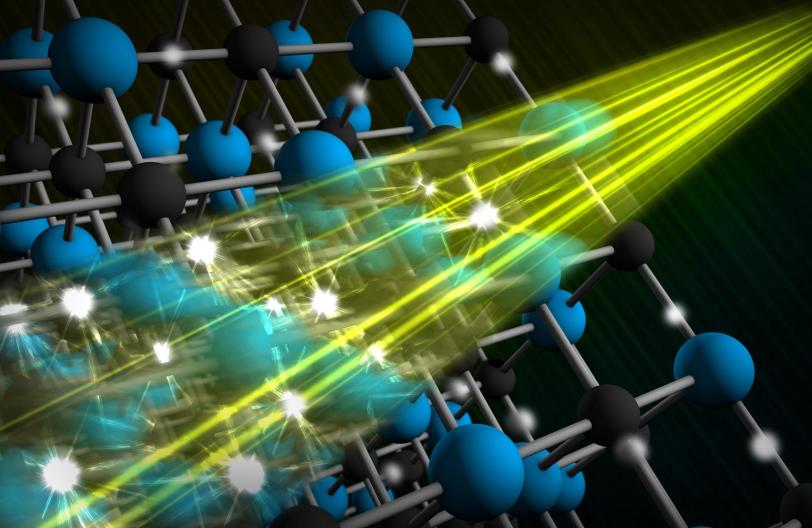
From hard to malleable, from transparent to opaque, from channeling electricity to blocking it: Materials come in all types. A number of their intriguing properties originate in the way a material’s electrons “dance” with its lattice of atomic nuclei, which is also in constant motion due to vibrations known as phonons.
This coupling between electrons and phonons determines how efficiently solar cells convert sunlight into electricity. It also plays key roles in superconductors that transfer electricity without losses, topological insulators that conduct electricity only on their surfaces, materials that drastically change their electrical resistance when exposed to a magnetic field, and more.
At the Department of Energy’s SLAC National Accelerator Laboratory, scientists can study these coupled motions in unprecedented detail with the world’s most powerful X-ray laser, the Linac Coherent Light Source (LCLS). LCLS is a DOE Office of Science User Facility.
“It has been a long-standing goal to understand, initiate and control these unusual behaviors,” says LCLS Director Mike Dunne. “With LCLS we are now able to see what happens in these materials and to model complex electron-phonon interactions. This ability is central to the lab’s mission of developing new materials for next-generation electronics and energy solutions.”
LCLS works like an extraordinary strobe light: Its ultrabright X-rays take snapshots of materials with atomic resolution and capture motions as fast as a few femtoseconds, or millionths of a billionth of a second. For comparison, one femtosecond is to a second what seven minutes is to the age of the universe.
Two recent studies made use of these capabilities to study electron-phonon interactions in lead telluride, a material that excels at converting heat into electricity, and chromium, which at low temperatures has peculiar properties similar to those of high-temperature superconductors.
Turning Heat into Electricity and Vice Versa
Lead telluride, a compound of the chemical elements lead and tellurium, is of interest because it is a good thermoelectric: It generates an electrical voltage when two opposite sides of the material have different temperatures.
“This property is used to power NASA space missions like the Mars rover Curiosity and to convert waste heat into electricity in high-end cars,” says Mariano Trigo, a staff scientist at the Stanford PULSE Institute and the Stanford Institute for Materials and Energy Sciences (SIMES), both joint institutes of Stanford University and SLAC. “The effect also works in the opposite direction: An electrical voltage applied across the material creates a temperature difference, which can be exploited in thermoelectric cooling devices.”
Mason Jiang, a recent graduate student at Stanford, PULSE and SIMES, says, “Lead telluride is exceptionally good at this. It has two important qualities: It’s a bad thermal conductor, so it keeps heat from flowing from one side to the other, and it’s also a good electrical conductor, so it can turn the temperature difference into an electric current. The coupling between lattice vibrations, caused by heat, and electron motions is therefore very important in this system. With our study at LCLS, we wanted to understand what’s naturally going on in this material.”
In their experiment, the researchers excited electrons in a lead telluride sample with a brief pulse of infrared laser light, and then used LCLS’s X-rays to determine how this burst of energy stimulated lattice vibrations.
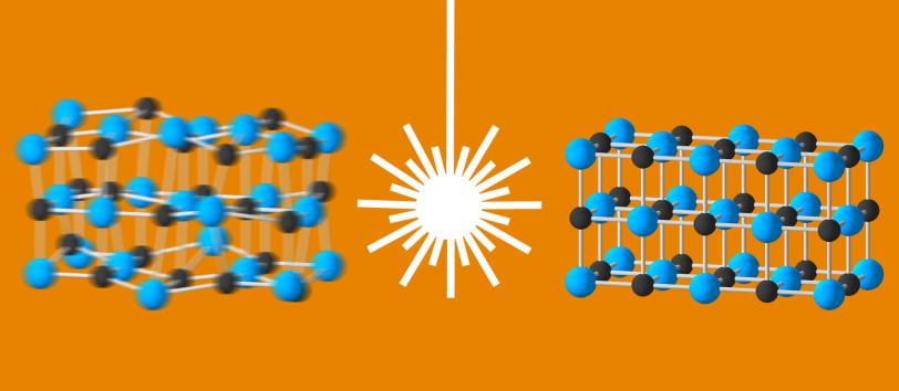
“Lead telluride sits at the precipice of a coupled electronic and structural transformation,” says principal investigator David Reis from PULSE, SIMES and Stanford. “It has a tendency to distort without fully transforming – an instability that is thought to play an important role in its thermoelectric behavior. With our method we can study the forces involved and literally watch them change in response to the infrared laser pulse.”
The scientists found that the light pulse excites particular electronic states that are responsible for this instability through electron-phonon coupling. The excited electrons stabilize the material by weakening certain long-range forces that were previously associated with the material’s low thermal conductivity.
“The light pulse actually walks the material back from the brink of instability, making it a worse thermoelectric,” Reis says. “This implies that the reverse is also true – that stronger long-range forces lead to better thermoelectric behavior.”
The researchers hope their results, published July 22 in Nature Communications, will help them find other thermoelectric materials that are more abundant and less toxic than lead telluride.
Controlling Materials by Stimulating Charged Waves
The second study looked at charge density waves – alternating areas of high and low electron density across the nuclear lattice – that occur in materials that abruptly change their behavior at a certain threshold. This includes transitions from insulator to conductor, normal conductor to superconductor, and from one magnetic state to another.
These waves don’t actually travel through the material; they are stationary, like icy waves near the shoreline of a frozen lake.
“Charge density waves have been observed in a number of interesting materials, and establishing their connection to material properties is a very hot research topic,” says Andrej Singer, a postdoctoral fellow in Oleg Shpyrko’s lab at the University of California, San Diego. “We’ve now shown that there is a way to enhance charge density waves in crystals of chromium using laser light, and this method could potentially also be used to tweak the properties of other materials.”
Laser pulse hitting a chromium crystal
This movie shows how a laser pulse hitting a chromium crystal causes charge density waves – alternating areas of high and low electron density within the crystal – to oscillate in height, or amplitude. The signal seen here is made by X-ray laser pulses scattering off the crystal. The timescale of the oscillations is shown in picoseconds, or trillionths of a second. (A. Singer/University of California, San Diego)
This could mean, for example, that scientists might be able to switch a material from a normal conductor to a superconductor with a single flash of light. Singer and his colleagues reported their results on July 25 in Physical Review Letters.
The research team used the chemical element chromium as a simple model system to study charge density waves, which form when the crystal is cooled to about minus 280 degrees Fahrenheit. They stimulated the chilled crystal with pulses of optical laser light and then used LCLS X-ray pulses to observe how this stimulation changed the amplitude, or height, of the charge density waves.
“We found that the amplitude increased by up to 30 percent immediately after the laser pulse,” Singer says. “The amplitude then oscillated, becoming smaller and larger over a period of 450 femtoseconds, and it kept going when we kept hitting the sample with laser pulses. LCLS provides unique opportunities to study such process because it allows us to take ultrafast movies of the related structural changes in the lattice.”
Based on their results, the researchers suggested a mechanism for the amplitude enhancement: The light pulse interrupts the electron-phonon interactions in the material, causing the lattice to vibrate. Shortly after the pulse, these interactions form again, which boosts the amplitude of the vibrations, like a pendulum that swings farther out when it receives an extra push.
A Bright Future for Studies of the Electron-Phonon Dance
Studies like these have a high priority in solid-state physics and materials science because they could pave the way for new materials and provide new ways to control material properties.
With its 120 ultrabright X-ray pulses per second, LCLS reveals the electron-phonon dance with unprecedented detail. More breakthroughs in the field are on the horizon with LCLS-II – a next-generation X-ray laser under construction at SLAC that will fire up to a million X-ray flashes per second and will be 10,000 times brighter than LCLS.
“LCLS-II will drastically increase our chances of capturing these processes,” Dunne says. “Since it will also reveal subtle electron-phonon signals with much higher resolution, we’ll be able to study these interactions in much greater detail than we can now.”
Other research institutions involved in the studies were University College Cork, Ireland; Imperial College London, UK; Duke University; Oak Ridge National Laboratory; RIKEN Spring-8 Center, Japan; University of Tokyo, Japan; University of Michigan; and University of Kiel, Germany. Funding sources included DOE Office of Science; Science Foundation Ireland; Volkswagen Foundation, Germany; and Federal Ministry of Education and Research, Germany. Preliminary X-ray studies on lead telluride were performed at SLAC’s Stanford Synchrotron Radiation Lightsource (SSRL), a DOE Office of Science User Facility, and at the Spring-8 Angstrom Compact Free-electron Laser (SACLA), Japan.
LCLS-II: The Next Leap for X-ray Science
Citations: M.P. Jiang et al., Nature Communications, 22 July 2016 (10.1038/ncomms12291); A. Singer et al., Physical Review Letters, 25 July 2016 (10.1103/PhysRevLett.117.056401).
For questions or comments, contact the SLAC Office of Communications at communications@slac.stanford.edu.
About SLAC
SLAC National Accelerator Laboratory explores how the universe works at the biggest, smallest and fastest scales and invents powerful tools used by researchers around the globe. As world leaders in ultrafast science and bold explorers of the physics of the universe, we forge new ground in understanding our origins and building a healthier and more sustainable future. Our discovery and innovation help develop new materials and chemical processes and open unprecedented views of the cosmos and life’s most delicate machinery. Building on more than 60 years of visionary research, we help shape the future by advancing areas such as quantum technology, scientific computing and the development of next-generation accelerators.
SLAC is operated by Stanford University for the U.S. Department of Energy’s Office of Science. The Office of Science is the single largest supporter of basic research in the physical sciences in the United States and is working to address some of the most pressing challenges of our time.
