Engineers Make World's Fastest Organic Transistor, Heralding New Generation of See-through Electronics
Teams from Stanford/SLAC and the University of Nebraska-Lincoln collaborate to make thin, transparent semiconductors that could become the foundation for cheap, high-performance displays.
By Tom Abate, Stanford Engineering
Two university research teams have worked together to produce the world’s fastest thin-film organic transistors, proving that this experimental technology has the potential to achieve the performance needed for high-resolution television screens and similar electronic devices.
For years engineers the world over have been trying to use inexpensive, carbon-rich molecules and plastics to create organic semiconductors capable of performing electronic operations at something approaching the speed of costlier technologies based on silicon. The term “organic” was originally confined to compounds produced by living organisms but now extended to include synthetic substances based on carbons and includes plastics.
In the Jan. 8 edition of Nature Communications, engineers from the University of Nebraska-Lincoln (UNL) and Stanford University show how they created thin-film organic transistors that could operate more than five times faster than previous examples of this experimental technology. Some of the work was performed by SLAC National Accelerator Laboratory researchers at the lab's Stanford Synchrotron Radiation Lightsource (SSRL).
The research teams were led by Zhenan Bao, professor of chemical engineering at Stanford and member of the Stanford Institute for Materials and Energy Sciences, which is run jointly with SLAC; and Jinsong Huang, assistant professor of mechanical and materials engineering at UNL. They used their new process to make organic thin-film transistors with electronic characteristics comparable to those found in expensive, curved-screen television displays based on a form of silicon technology.
They achieved their speed boost by altering the basic process for making thin-film organic transistors.
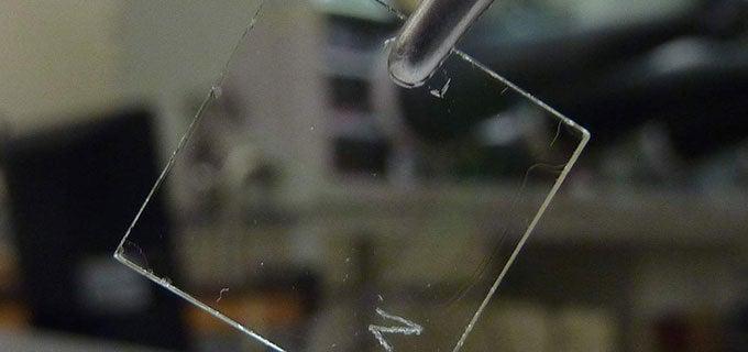
Typically, researchers drop a special solution, containing carbon-rich molecules and a complementary plastic, onto a spinning platter – in this case, one made of glass. The spinning action deposits a thin coating of the materials over the platter.
In their Nature Communications paper, the collaborators describe two important changes to this basic process.
First they spun the platter faster. Second they only coated a tiny portion of the spinning surface, equivalent to the size of a postage stamp.
These innovations had the effect of depositing a denser concentration of the organic molecules into a more regular alignment. The result was a great improvement in carrier mobility, which measures how quickly electrical charges travel through the transistor.
The researchers called this improved method “off-center spin coating.” The process remains experimental, and the engineers cannot yet precisely control the alignment of organic materials in their transistors or achieve uniform carrier mobility.
Even at this stage, off-center spin coating produced transistors with a range of speeds much faster than those of previous organic semiconductors and comparable to the performance of the polysilicon materials used in today’s high-end electronics.
Further improvements to this experimental process could lead to the development of inexpensive, high-performance electronics built on transparent substrates such as glass and, eventually, clear and flexible plastics.
Already, the researchers have shown that they can create high-performance organic electronics that are 90 percent transparent to the naked eye.
Other key members of the research teams included Yongbo Yuan, a postdoctoral associate at UNL’s Nebraska Center for Materials and Nanoscience, Gaurav Giri, a graduate student in chemical engineering at Stanford and Alex Ayzner, a postdoctoral researcher at SSRL. SSRL's Stefan Mannsfeld, Dennis Nordlund and Michael Toney also contributed to the research.
The work was funded by the U.S. Defense Advanced Research Projects Agency (DARPA), the Air Force Office of Scientific Research and the National Science Foundation.
This article originally appeared on the Stanford School of Engineering website. Tom Abate is a science writer and Associate Director of Communications at Stanford Engineering. Carole Wilbeck of the UNL College of Engineering also contributed to this report.
Media Contacts
Tom Abate, Associate Director of Communications at Stanford Engineering, 650-736-2245, tabate@stanford.edu
Jinsong Huang, Assistant Professor, Mechanical and Materials Engineering, University of Nebraska-Lincoln, 402-472-2640, jhuang2@unl.edu

Related stories