SLAC topics

Stanford Institute for Materials & Energy Sciences (SIMES) RSS feed

SIMES researchers study complex, novel materials that could transform the energy landscape by making computing much more efficient or transmitting power over long distances with no loss, for instance.

Visit SIMES website

Browse tagged content below
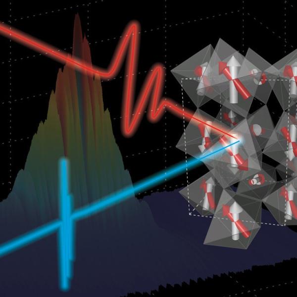
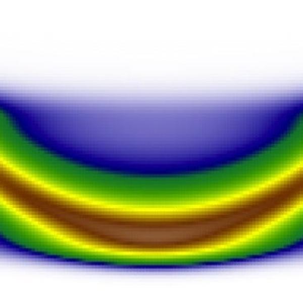
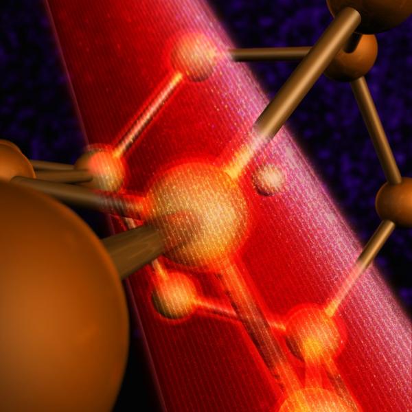
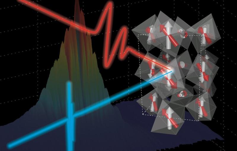
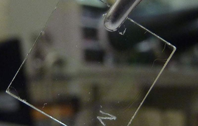
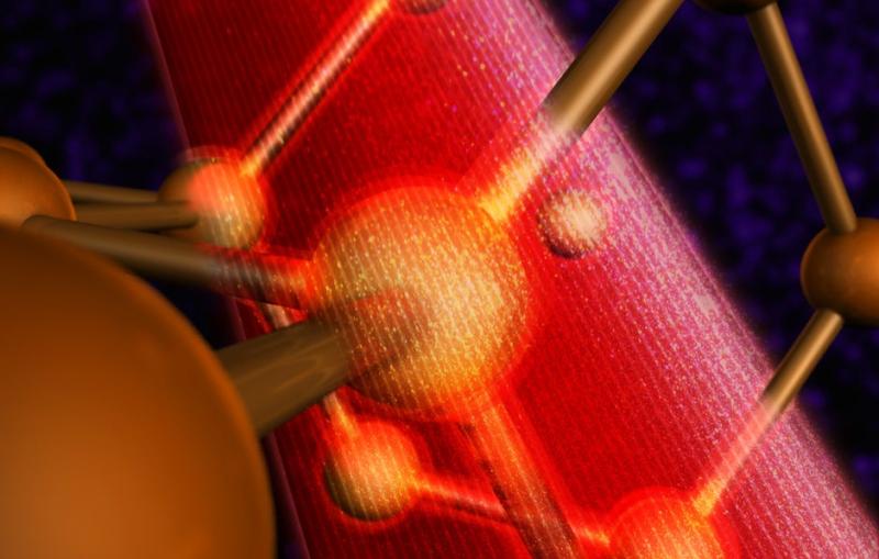
Polarons, bubbles of distortion in a perovskite lattice.
Feature

SLAC's Siegfried Glenzer has been selected to receive an Ernest Orlando Lawrence Award, presented by the U.S. Secretary of Energy to honor scientists across...

Photo - Siegfried Glenzer
Feature

A new theory and computer simulation by SLAC and Stanford researchers rule out high-energy magnetic interactions as a major factor in making copper oxide...

Photo - Researchers at SLAC
Feature

SLAC researchers have found a new way to transform graphite into diamond. The approach may have implications for industrial applications ranging from cutting tools...

News Release

Scientists have discovered a potential way to make graphene – a single layer of carbon atoms with great promise for future electronics – superconducting...

Superconducting Graphene Layers
Feature

An experiment at SLAC’s X-ray laser has revealed the first atomic-scale details of a new technique that could point the way to faster data...

Image - A laser-driven electric pulse excites a magnetic response in a multiferroic material that is measured by SLAC's X-ray laser pulse (blue).
News Release

An electrode designed like a pomegranate – with silicon nanoparticles clustered like seeds in a tough carbon rind – overcomes several remaining obstacles to...

A fanciful illustration of pomegranate seeds inside a conventional battery
Feature

Jolting complex materials with bursts of energy from rapid-fire lasers can help scientists learn why some of these materials exhibit useful properties such as...

Image - Pictured is the initial, equilibrium distribution of electron energy after an intense pulse of near-infrared light. (SIMES)
Feature

While this particular material is very unstable, the research shows it may be possible to find a material with the properties graphene has to...

photo of zhongkai liu
Feature

Crafted in a single atomic layer, it could be a natural fit for making thin, flexible light-based electronics, as well as futuristic 'spintronics' and...

This diagram shows a single layer of MoSe2 thin film (green and yellow balls) grown on a layer of graphene (black balls) that has formed on the surface of a silicon carbide substrate. (Yi Zhang, SIMES and ALS/Berkeley Lab)
Feature

Teams from Stanford, SLAC and the University of Nebraska-Lincoln collaborate to make thin, transparent semiconductors that could become the foundation for cheap, high-performance displays.

See caption
Feature

An international team led by scientists from two SLAC/Stanford institutes has devised a much faster and more accurate way of measuring subtle atomic vibrations...

Image showing laser beam energizing atoms in crystal lattic
News Release

A single layer of tin atoms could be the world’s first material to conduct electricity with 100 percent efficiency at the temperatures that computer...

Photo - tin can and piece of scrap tin sitting on a periodic table of elements with tin "Sn" highlighted