Scientists from SIMES and Berkeley Lab Cook Up New Electronic Material
Crafted in a single atomic layer, it could be a natural fit for making thin, flexible light-based electronics, as well as futuristic 'spintronics' and 'valleytronics.'
By Glennda Chui
Scientists from SLAC, Stanford and Berkeley Lab grew sheets of an exotic material in a single atomic layer and measured its electronic structure for the first time. They discovered it’s a natural fit for making thin, flexible light-based electronics.
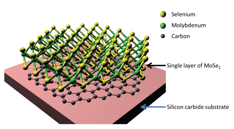
In a study published Dec. 22 in Nature Nanotechnology, the researchers give a recipe for making the thinnest possible sheets of the material, called molybdenum diselenide or MoSe2, in a precisely controlled way, using a technique that’s common in electronics manufacturing.
“We found the right recipe, and we provide it in the paper so people can develop it more for industrial purposes,” said Sung-Kwan Mo, a beam scientist at Lawrence Berkeley National Laboratory’s Advanced Light Source (ALS), where the material was made.
“Based on tests at the ALS and at Stanford, now we can say MoSe2 has possible applications in photoelectronic devices, such as light detectors and solar cells,” said Yi Zhang, a postdoctoral researcher who designed and built the equipment used to make the thin sheets, and the report’s first author. The material also has potential for novel types of electronics that are still in the future, he said. Zhang is affiliated with Berkeley Lab and the Stanford Institute for Materials and Energy Sciences, which is jointly run with SLAC National Accelerator Laboratory.
Single atomic sheets of MoSe2 have been generating a lot of scientific interest lately because they belong to a small class of materials that absorb light and glow with great efficiency.
But until now, no one had been able to make extremely thin layers of MoSe2 in significant quantities and directly observe the evolution of their electronic structure. This is important because a material’s electronic behavior can change fundamentally, and in useful ways, when its electrons are confined to such thin layers.
To make the sheets, researchers heated molybdenum and selenium in a vacuum chamber at the ALS until they evaporated. The two elements combined and were deposited as a thin, high-quality film. By tweaking the process, known as molecular beam epitaxy, the scientists were able to grow films that were one to eight atomic layers thick.
The team probed the electronic structure of the film with the ALS’s powerful X-ray beam, and later with equipment at Stanford. They found the first direct experimental evidence that the material abruptly changes electronic structure, becoming a much more efficient absorber and emitter of visible light, when made in sheets that are atomically thin.
The team also discovered that electrons with different spins – described as either “up” or “down” – travel along different paths and in opposite directions through the hexagonal structure of single-layer MoSe2. This could prove useful in “spintronics,” a next-generation technology that would use the spins of electrons, rather than their charge, to carry and store information, said Yongtao Cui, a Stanford postdoctoral researcher who was involved in testing the film.
MoSe2’s novel structure may also lend itself to an even newer concept called “valleytronics,” in which both spin and charge are used to transport and store information. This idea surfaced in 2002; like spintronics, it’s being eagerly explored as a potential way to continue the trend toward smaller, faster, cheaper electronic devices.
“This field is still in the initial stage of development,” Cui said. “People have these applications in mind, but as research goes along they may discover new aspects of these materials, and possibly new applications.”
The research was led by Zhi-Xun Shen, a professor at SLAC and Stanford and SLAC’s advisor for science and technology. Collaborators included other scientists from Stanford, SLAC and Berkeley Lab, as well as from National Tsing Hua University in Taiwan, the University of Oxford in the United Kingdom and Northeastern University in Boston.
Work at the ALS, Stanford and Northeastern University was supported by the U.S. Department of Energy’s Office of Basic Energy Science, and the work at Oxford was supported by the Defense Advanced Research Projects Agency (DARPA) Mesodynamic Architectures program.
Published online: 22 December 2013 | doi:10.1038/nnano.2013.277
Contact
For questions or comments, contact the SLAC Office of Communications at communications@slac.stanford.edu.
SLAC is a multi-program laboratory exploring frontier questions in photon science, astrophysics, particle physics and accelerator research. Located in Menlo Park, California, SLAC is operated by Stanford University for the U.S. Department of Energy Office of Science. To learn more, please visit www.slac.stanford.edu.
The Stanford Institute for Materials and Energy Sciences (SIMES) is a joint institute of SLAC National Accelerator Laboratory and Stanford University. SIMES studies the nature, properties and synthesis of complex and novel materials in the effort to create clean, renewable energy technologies. For more information, please visit simes.slac.stanford.edu.
Lawrence Berkeley National Laboratory’s Advanced Light Source is a third-generation synchrotron light source producing light in the X-ray region of the spectrum that is a billion times brighter than the sun. A DOE national user facility, the ALS attracts scientists from around the world and supports its users in doing outstanding science in a safe environment. For more information visit www-als.lbl.gov.
DOE's Office of Science is the largest supporter of basic research in the physical sciences in the United States, and is working to address some of the most pressing challenges of our time. For more information, please visit science.energy.gov.
Related stories