A Record-setting Way to Make Transparent Conductors: Spread Them Like Butter on Toast
Stanford, SLAC Process Has Potential for Scaling Up to Manufacture Solar Cells, Displays and More
Scientists from Stanford University and the Department of Energy’s SLAC National Accelerator Laboratory have shown they can make flexible, transparent electrical conductors with record-high performance for use in solar cells, displays and other devices by spreading polymers on a clear surface with a tiny blade, like a knife spreading butter on toast.
The technique, reported Oct. 29 in the advance online edition of Proceedings of the National Academy of Sciences, has already been used to make patterned electrodes for touch sensors and organic solar cells, and with further development could be a tool for manufacturing transparent conductors on a large scale.
“We were able to achieve record-high conductivity with a material people have known for years, just by tuning the coating process,” said Zhenan Bao, a Stanford professor and member of SIMES, the Stanford Institute for Materials and Energy Sciences at SLAC, who led the study. “That shows there’s a lot of room for achieving high performance through controlling the assembly and structure of materials at the molecular scale.”
Clear Conductors for Flexible Gadgets
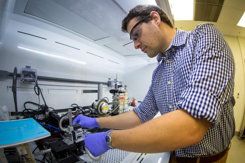
Bao’s group developed this “solution shearing” technique in close collaboration with Michael Toney and Stefan Mannsfeld, staff scientists at SLAC’s Stanford Synchrotron Radiation Lightsource (SSRL), whose teams used X-rays to look at the structures and properties of the finished films.
Transparent conductors are used where it’s important to get light in or out of a device, such as in solar cells, electromagnetic shielding, antistatic layers and lighting displays. Today these conductors are mostly made with indium tin oxide, or ITO. But ITO is expensive to work with, and it isn’t compatible with the flexible displays being developed for a new generation of TV screens, computers and other electronics.
“There’s a huge drive in industry to create things that are transparent, inexpensive, conduct well and are made from abundant materials,” said Mannsfeld, who is now a professor at the Dresden University of Technology.
So, scientists have been exploring alternatives. In this study they turned to PEDOT:PSS, a conductive blend of two polymers that turns transparent as it dries. It’s also much cheaper and more flexible than ITO.
Tuning the Process Yields Record Results
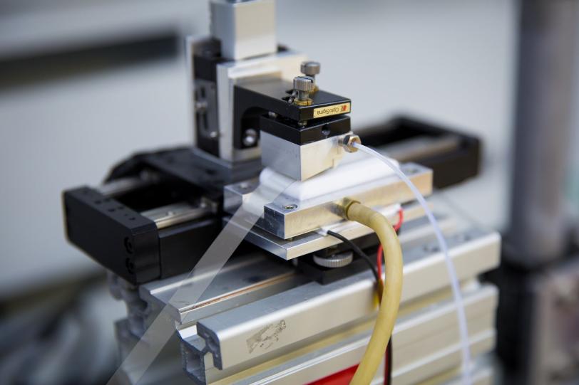
A matchbook-sized silicon blade spread a thin layer of PEDOT:PSS on various surfaces – including glass, silicon, and PET, a clear polyester resin used in beverage containers – at speeds up to 6 meters per minute. By varying the speed and adjusting the temperature of this process, the researchers were able to produce see-through films of various thickness and conductivity, and also get the PEDOT and PSS polymers to separate into layers, which increased the film’s conductivity even more. The best films they made beat the existing conductivity record for PEDOT:PSS.
Next they used the method to create working electrodes: First they printed electronic circuit patterns on a glass surface with a chip manufacturing technique called photolithography. Then they spread the polymer mix over the surface with the blade. The conductive polymers stuck to the patterned areas but not to the bare glass, creating circuits where electrical currents can travel. The resulting electrodes were tested and found to work in solar cells and touch sensors.
“Solution shearing is still an experimental technique, but it’s becoming more common as a way to deposit these polymeric materials,” said Sean Andrews, a postdoctoral researcher who carried out the bulk of the experiments with former postdoc Brian Worfolk, now a scientist with Phillips 66. “We’re looking for ways to increase the performance of these films with methods that can be scaled up for industrial manufacturing.”
He said the team continues to carry out X-ray studies to find out exactly why spreading the polymers with a blade – which stretches them out along one direction and arranges the molecules in different ways as they dry – makes them more conductive, so they can control and take advantage of the process to make even better transparent conductors.
In earlier studies, the research team used variations of the technique to test better ways to manufacture high-quality semiconductors and solar cells. Their solution shearing apparatus was set up with funding from a SLAC Laboratory Directed Research and Development grant. The research was also supported by the DOE’s Energy Efficiency and Renewable Energy (EERE) BRIDGE program, which aims to significantly lower the cost of solar energy systems; the Stanford Global Climate and Energy Program; Stanford’s Tomkat Center for Sustainable Energy; and the National Science Foundation. Parts of the study were carried out at SSRL, which is a DOE Office of Science User Facility.
Citation: B. Worfolk et al., Proceedings of the National Academy of Sciences, 29 October 2015 (10.1073/pnas.1509958112)
For questions or comments, contact the SLAC Office of Communications at communications@slac.stanford.edu.
SLAC is a multi-program laboratory exploring frontier questions in photon science, astrophysics, particle physics and accelerator research. Located in Menlo Park, Calif., SLAC is operated by Stanford University for the U.S. Department of Energy's Office of Science.
SLAC National Accelerator Laboratory is supported by the Office of Science of the U.S. Department of Energy. The Office of Science is the single largest supporter of basic research in the physical sciences in the United States, and is working to address some of the most pressing challenges of our time. For more information, please visit science.energy.gov.