Ultrafast electrons and lasers open possibilities for better imaging and sensing technologies
SLAC and Stanford scientists used ultrafast electrons and a laser to reveal an unexpectedly strong optical response to ionization, opening new possibilities for radiological imaging and sensing while shedding light on the fundamental behavior of materials.
By Emily Ayshford
Key takeaways:
- A SLAC/Stanford University research team sent charged electrons into semiconductor samples, then used ultrafast laser pulses to optically probe the result.
- Not only could the researchers detect high-energy particles in real time, they also found that the charge carriers within the material were crowded together in local, dense pockets, changing how semiconductors absorbed and transmitted light.
- The results could have implications in medical imaging and sensing technologies.

Detecting radiation is key to technologies ranging from particle accelerators and scientific instruments to medical imaging and security screening.
But current detectors must often make tradeoffs, providing signals that are strong but slow or fast but weak. The tradeoff between signal strength and speed can limit precision detection.
In new research, Stanford University researchers worked with the Department of Energy’s SLAC National Accelerator Laboratory on a unique experimental set-up to detect radiation across a range of materials.
What they found surprised them. Not only did the researchers observe an unexpectedly strong, ultrafast radiation signals, they also found that the charge within the materials acted differently than expected.
The research, published in the journal Nature Photonics, revealed new insights about the behavior of materials while potentially paving the way for better sensing technologies.
Harnessing the power of MeV-UED
Radiation that frees electrons from atoms – called ionizing radiation – penetrates deep within structures, allowing us to peer inside materials and the human body.
Because it cannot be measured directly, researchers instead detect it through secondary signals, such as light or electrical signals, that are generated when ionizing radiation interacts with matter. These secondary signals, however, are often either strong but slow to develop, or fast but provide a weak response.
Diana Jeong, instructor of radiology at Stanford University and corresponding author of the research, set out to systematically investigate the optical signal strengths generated across a range of material classes induced by ionization. By understanding these signals generated by light waves, she wondered if she could find a detection method that would provide better tradeoffs.
Most radiation detectors today rely on scintillators, materials that absorb radiation and convert it into visible light. During a PET scan, for example, patients are injected with a small amount of radioactive tracer. As the tracer decays, it emits particles called positrons that ultimately emit radiation in the form of gamma rays, which are detected by scintillator crystals.
“When the radiation hits the scintillator, it glows,” Jeong said. "That glow has been the standard signal for radiation detection for decades. But because it develops over time, we wondered whether there was an earlier light signal immediately after ionization that we could observe with ultrafast laser pulses."
Instructor of Radiology, Stanford UniversityWe wondered whether there was an earlier light signal immediately after ionization that we could observe with ultrafast laser pulses.
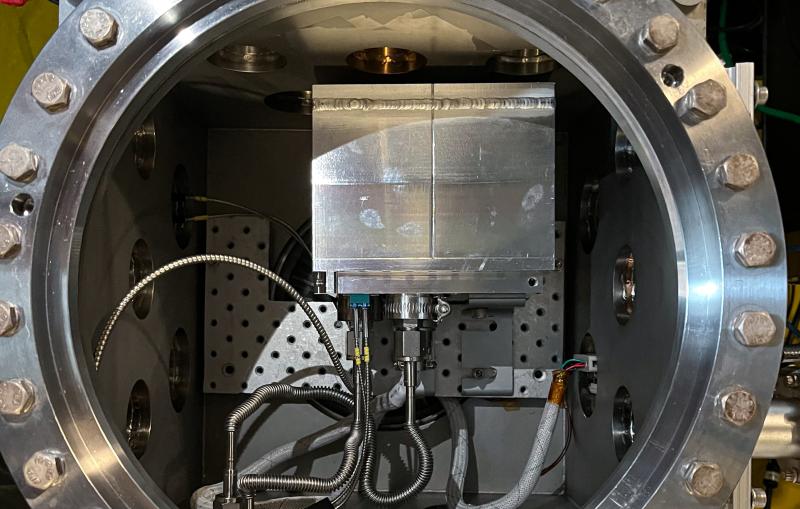
To answer that question, Jeong used the Megaelectronvolt Ultrafast Electron Diffraction (MeV-UED) instrument at SLAC’s Linac Coherent Light Source (LCLS). The system is a powerful “electron camera” that uses electrons to study atomic and molecular dynamics.
In this case, Jeong didn’t want to use the electrons to image samples – she wanted to deposit high-energy electrons into the sample so she could detect the resulting changes with lasers across different wavelengths, leveraging the unique capabilities of SLAC's MeV-UED facility.
“Normally, we use this system to measure electron diffraction, but this experiment flipped that on its head,” said Patrick Kramer, a SLAC staff scientist and the laser science lead for MeV-UED. “It’s a microscopy experiment in a different sense.”
SLAC Staff ScientistNormally, we use this system to measure electron diffraction, but this experiment flipped that on its head.
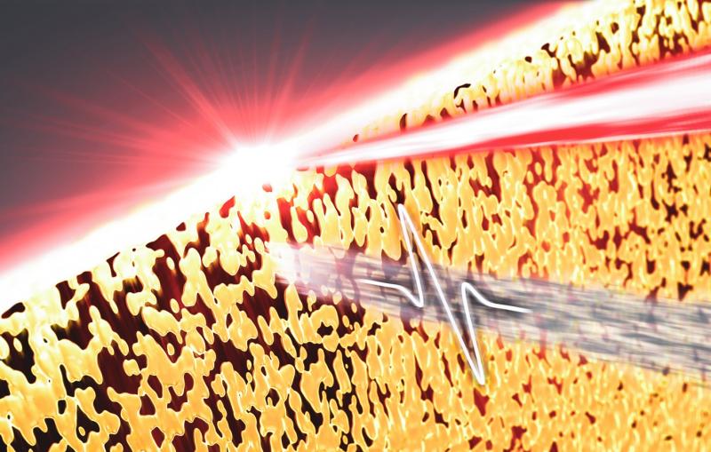
The high-energy electrons emulate ionization processes found in applications such as PET imaging, depositing energy into the sample. But instead of detecting the glow, the synchronized laser pulses probed the material's optical response immediately after ionization.
To explore how different materials respond on these ultrafast timescales, Jeong and her collaborators studied II-VI semiconductors – a family of common semiconductor materials that are used across electronic applications, including infrared detectors and photovoltaic solar cells.
“Semiconductors are ideal for a proof-of-concept experiment like this, because they essentially convert this high-energy radiation from electrons into measurable changes in their optical properties,” said Tom Hopper, an assistant professor of chemistry at the University of Central Florida who was a postdoctoral scholar at SLAC during this research.
A new understanding of material behavior
The experiment worked: The team had a strong signal and could see ultrafast changes within the semiconductors. But those changes surprised them and gave them new information on how materials behave under these conditions.
The team had expected the charge generated from the electrons to be distributed evenly throughout the sample. But instead, the charge carriers – electron-hole pairs that have been knocked off atoms – were crowded together in local, dense pockets. In other words, if the charge carriers were chocolate, Jeong had expected the experiment to produce a chocolate brownie, but instead it created a chocolate chip cookie.
“It was very weird,” she said. “The densities were much higher than we calculated.”
These dense bursts shifted the band gap of the materials – the energy range in materials where no electronic states exist – which changed how the semiconductors absorbed and transmitted light.
“The semiconductor was now able to transmit light where it normally would not be able to because the band gap shifted quite substantially in energy due to some process that has been driven by these high-energy electrons,” Hopper said.
Having this understanding of how high-energy electrons affect samples – and provide strong signals through these dense pockets of energy – could help researchers develop advanced sensing technologies.
Jeong believes these effects would show up at lower-energy systems – like imaging systems that could potentially be used at a physician’s office – as well. That could ultimately lead to new imaging technologies capable of real-time disease monitoring and diagnosis.
“Our hope is that this leads to new sensing platforms that can form images right away and lead to real-time intervention,” Jeong said.
This work was supported by the DOE Office of Science. LCLS is an Office of Science user facility. Additional support was provided by the National Science Foundation and the National Institutes of Health.
Citation: D. Jeong et al., Nature Photonics, 20 April 2026 (10.1038/s41566-026-01894-3)
For media inquiries, please contact media@slac.stanford.edu. For other questions or comments, contact SLAC Strategic Communications & External Affairs at communications@slac.stanford.edu.
About SLAC
SLAC National Accelerator Laboratory explores how the universe works at the biggest, smallest and fastest scales and invents powerful tools used by researchers around the globe. As world leaders in ultrafast science and bold explorers of the physics of the universe, we forge new ground in understanding our origins and building a healthier and more sustainable future. Our discovery and innovation help develop new materials and chemical processes and open unprecedented views of the cosmos and life’s most delicate machinery. Building on more than 60 years of visionary research, we help shape the future by advancing areas such as quantum technology, scientific computing and the development of next-generation accelerators.
SLAC is operated by Stanford University for the U.S. Department of Energy’s Office of Science. The Office of Science is the single largest supporter of basic research in the physical sciences in the United States and is working to address some of the most pressing challenges of our time.