Scientists uncover a process that stands in the way of making quantum dots brighter
The results have important implications for today’s TV and display screens and for future technologies where light takes the place of electrons and fluids.
By Glennda Chui
Bright semiconductor nanocrystals known as quantum dots give QLED TV screens their vibrant colors. But attempts to increase the intensity of that light generate heat instead, reducing the dots’ light-producing efficiency.
A new study explains why, and the results have broad implications for developing future quantum and photonics technologies where light replaces electrons in computers and fluids in refrigerators, for example.
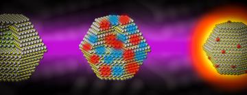
In a QLED TV screen, dots absorb blue light and turn it into green or red. At the low energies where TV screens operate, this conversion of light from one color to another is virtually 100% efficient. But at the higher excitation energies required for brighter screens and other technologies, the efficiency drops off sharply. Researchers had theories about why this happens, but no one had ever observed it at the atomic scale until now.
To find out more, scientists at the Department of Energy’s SLAC National Accelerator Laboratory used a high-speed “electron camera” to watch dots turn incoming high-energy laser light into their own glowing light emissions.
The experiments revealed that the incoming high-energy laser light ejects electrons from the dot’s atoms, and their corresponding holes – empty spots with positive charges that are free to move around – become trapped at the surface of the dot, producing unwanted waste heat.
In addition, electrons and holes recombine in a way that gives off additional heat energy. This increases the jiggling of the dot’s atoms, deforms its crystal structure and wastes even more energy that could have gone into making the dots brighter.
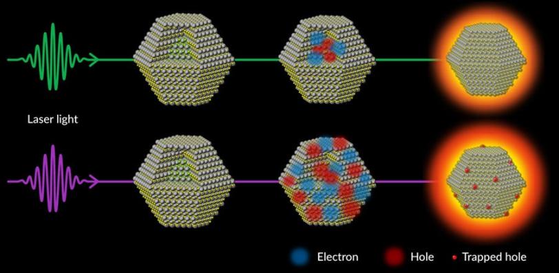
The results have broad implications for developing future quantum and photonics technologies where light replaces electrons in computers and fluids in refrigerators. (B. Guzelturk et al., Nature Communications, 25 March 2021)
“This represents a key way that energy is sucked out of the system without giving rise to light,” said Aaron Lindenberg, a Stanford University associate professor and investigator with the Stanford Institute for Materials and Energy Sciences at SLAC who led the study with postdoctoral researcher Burak Guzelturk.
"Trying to figure out what underlies this process has been the subject of study for decades,” he said. “This is the first time we could see what the atoms are actually doing while excited state energy is being lost as heat.”
The research team, which included scientists from SLAC, Stanford, the University of California, Berkeley and DOE’s Lawrence Berkeley National Laboratory, described the results in Nature Communications today.
Emitting a pure, brilliant glow
Despite their tiny size – they have about the same diameter as four strands of DNA – quantum dot nanocrystals are surprisingly complex and highly engineered. They emit extremely pure light whose color can be tuned by adjusting their size, shape, composition and surface chemistry. The quantum dots used in this study were invented more than two decades ago, and today they’re widely used in bright, energy-efficient displays and in imaging tools for biology and medicine.
Understanding and fixing problems that stand in the way of making dots more efficient at higher energies is a very hot field of research right now, said Guzelturk, who carried out experiments at SLAC with postdoctoral researcher Ben Cotts.
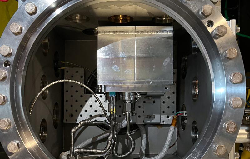
Previous studies had focused on how the dots’ electrons behaved. But in this study, the team was able to see the movements of whole atoms, too, with an electron camera known as MeV-UED. It hits samples with short pulses of electrons with very high energies, measured in millions of electronvolts (MeV). In a process called ultrafast electron diffraction (UED), the electrons scatter off the sample and into detectors, creating patterns that reveal what both electrons and atoms are doing.
As the SLAC/Stanford team measured the behavior of quantum dots that had been hit with various wavelengths and intensities of laser light, UC Berkeley graduate students Dipti Jasrasaria and John Philbin worked with Berkeley theoretical chemist Eran Rabani to calculate and understand the resulting interplay of electronic and atomic motions from a theoretical standpoint.
“We met with the experimenters quite often,” Rabani said. “They came with a problem and we started to work together to understand it. Thoughts were going back and forth, but it was all seeded from the experiments, which were a big breakthrough in being able to measure what happens to the quantum dots’ atomic lattice when it’s intensely excited.”
A future of light-based technology
The study was carried out by researchers in a DOE Energy Frontier Research Center, Photonics at Thermodynamic Limits, led by Jennifer Dionne, a Stanford associate professor of materials science and engineering and senior associate vice provost of research platforms/shared facilities. Her research group worked with Lindenberg’s group to help develop the experimental technique for probing the nanocrystals.
The center’s ultimate goal, Dionne said, is to demonstrate photonic processes, such as light absorption and emission, at the limits of what thermodynamics allows. This could bring about technologies like refrigeration, heating, cooling and energy storage – as well as quantum computers and new engines for space exploration – powered entirely by light.
"To create photonic thermodynamic cycles, you need to precisely control how light, heat, atoms, and electrons interact in materials,” Dionne said. “This work is exciting because it provides an unprecedented lens on the electronic and thermal processes that limit the light emission efficiency. The particles studied already have record quantum yields, but now there is a path toward designing almost-perfect optical materials.” Such high light emission efficiencies could open a host of big futuristic applications, all driven by tiny dots probed with ultrafast electrons.
This work is part of the Photonics at Thermodynamic Limits Energy Frontier Research Center, funded by the DOE Office of Science. MeV-UED is operated as part of SLAC’s Linac Coherent Light Source, a DOE Office of Science user facility. Parts of the work were performed at the Center for Nanoscale Materials, a DOE Office of Science user facility at Argonne National Laboratory, and at the Stanford Nano Shared Facilities.
Citation: Burak Guzelturk et al., Nature Communications, 25 March 2020 (10.1038/s41467-021-22116-0)
For questions or comments, contact the SLAC Office of Communications at communications@slac.stanford.edu.
SLAC is a vibrant multiprogram laboratory that explores how the universe works at the biggest, smallest and fastest scales and invents powerful tools used by scientists around the globe. With research spanning particle physics, astrophysics and cosmology, materials, chemistry, bio- and energy sciences and scientific computing, we help solve real-world problems and advance the interests of the nation.
SLAC is operated by Stanford University for the U.S. Department of Energy’s Office of Science. The Office of Science is the single largest supporter of basic research in the physical sciences in the United States and is working to address some of the most pressing challenges of our time.
