Researchers add a ‘twist’ to classical material design
They’ve discovered that crystals can twist when they are sandwiched between two substrates – a critical step toward exploring new material properties for electronics and other applications.
By David Krause
Researchers with the Department of Energy’s SLAC National Accelerator Laboratory, Stanford University and the DOE's Lawrence Berkeley National Laboratory (LBNL) grew a twisted multilayer crystal structure for the first time and measured the structure’s key properties. The twisted structure could help researchers develop next-generation materials for solar cells, quantum computers, lasers and other devices.
“This structure is something that we have not seen before – it was a huge surprise to me,” said Yi Cui, a professor at Stanford and SLAC and paper co-author. “A new quantum electronic property could appear within this three-layer twisted structure in future experiments.”
Adding layers, with a twist
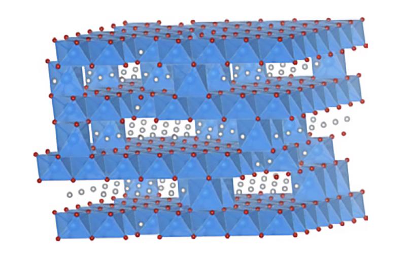
The crystals the team designed extended the concept of epitaxy, a phenomenon that occurs when one type of crystal material grows on top of another material in an ordered way – kind of like growing a neat lawn on top of soil, but at the atomic level. Understanding epitaxial growth has been critical to the development of many industries for more than 50 years, particularly the semiconductor industry. Indeed, epitaxy is part of many of the electronic devices that we use today, from cell phones to computers to solar panels, allowing electricity to flow, and not flow, through them.
To date, epitaxy research has focused on growing one layer of material onto another, and the two materials have the same crystal orientation at the interface. This approach has been successful for decades in many applications, such as transistors, light-emitting diodes, lasers and quantum devices. But to find new materials that perform even better for more demanding needs, like quantum computing, researchers are searching for other epitaxial designs – ones that might be more complex, yet better performing, hence the "twisted epitaxy" concept demonstrated in this study.
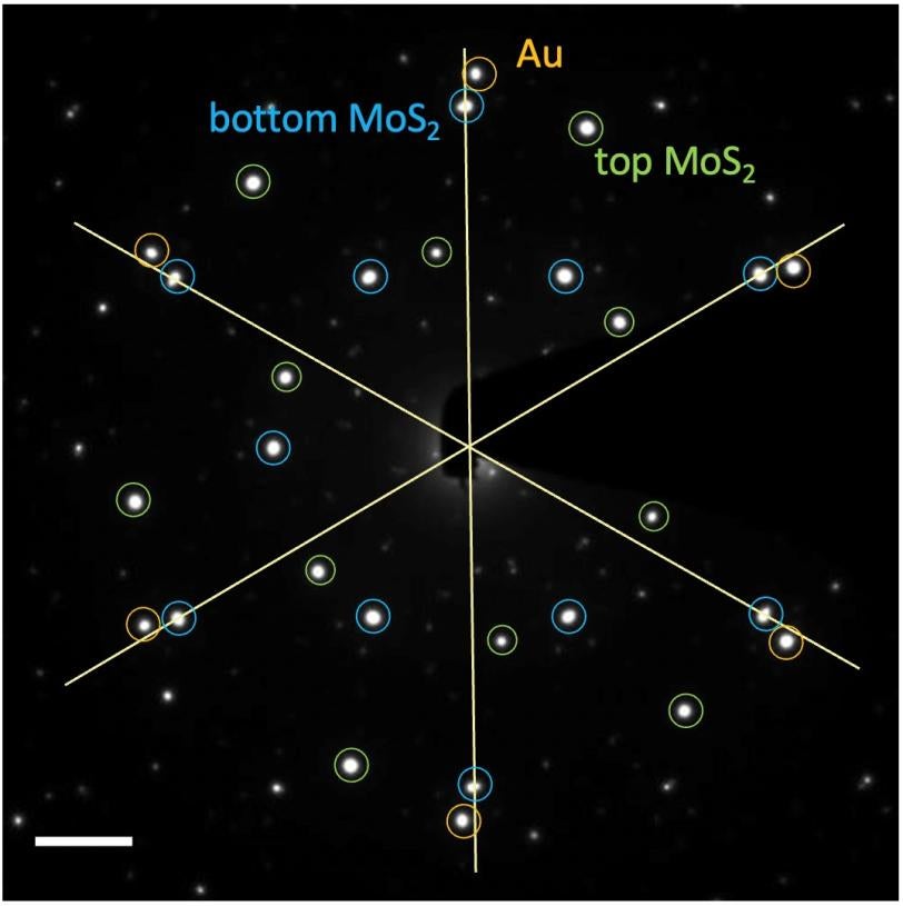
In their experiment, detailed this month in Science, researchers added a layer of gold between two sheets of a traditional semiconducting material, molybdenum disulfide (MoS2). Because the top and bottom sheets were oriented differently, the gold atoms could not align with both simultaneously, which allowed the Au structure to twist, said Yi Cui, Professor Cui's graduate student in materials science and engineering at Stanford and co-author of the paper.
“With only a bottom MoS2 layer, the gold is happy to align with it, so no twist happens,” said Cui, the graduate student. “But with two twisted MoS2 sheets, the gold isn’t sure to align with the top or bottom layer. We managed to help the gold solve its confusion and discovered a relationship between the orientation of Au and the twist angle of bilayer MoS2.”
Zapping gold nanodiscs
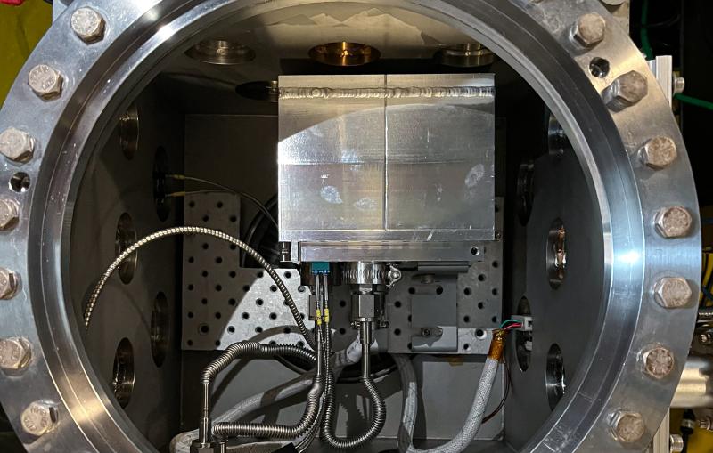
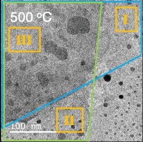
To study the gold layer in detail, the researcher team from the Stanford Institute for Materials and Energy Sciences (SIMES) and LBNL heated a sample of the whole structure to 500 degrees Celsius. Then they sent a stream of electrons through the sample using a technique called transmission electron microscopy (TEM), which revealed the morphology, orientation and strain of the gold nanodiscs after annealing at the different temperatures. Measuring these properties of the gold nanodiscs was a necessary first step toward understanding how the new structure could be designed for real world applications in the future.
“Without this study, we would not know if twisting an epitaxial layer of metal on top of a semiconductor was even possible,” said Cui, the graduate student. “Measuring the complete three-layer structure with electron microscopy confirmed that it was not only possible, but also that the new structure could be controlled in exciting ways.”
Next, researchers want to further study the optical properties of the gold nanodiscs using TEM and learn if their design alters physical properties like band structure of Au. They also want to extend this concept to try to build three-layer structures with other semiconductor materials and other metals.
“We’re beginning to explore whether only this combination of materials allows this or if it happens more broadly,” said Bob Sinclair, the Charles M. Pigott Professor in Stanford’s school of Materials Science and Engineering and paper co-author. “This discovery is opening a whole new series of experiments that we can try. We could be on our way to finding brand new material properties that we could exploit.”
Funding for this study came from the DOE Office of Science’s Basic Energy Sciences.
Citation: Cui et al., Science, 12 January 2024 (10.1126/science.adk5947)
About SLAC
SLAC National Accelerator Laboratory explores how the universe works at the biggest, smallest and fastest scales and invents powerful tools used by researchers around the globe. As world leaders in ultrafast science and bold explorers of the physics of the universe, we forge new ground in understanding our origins and building a healthier and more sustainable future. Our discovery and innovation help develop new materials and chemical processes and open unprecedented views of the cosmos and life’s most delicate machinery. Building on more than 60 years of visionary research, we help shape the future by advancing areas such as quantum technology, scientific computing and the development of next-generation accelerators.
SLAC is operated by Stanford University for the U.S. Department of Energy’s Office of Science. The Office of Science is the single largest supporter of basic research in the physical sciences in the United States and is working to address some of the most pressing challenges of our time.