In a first, scientists precisely measure how synthetic diamonds grow
A SLAC-Stanford study reveals exactly what it takes for diamond to crystallize around a “seed” cluster of atoms. The results apply to industrial processes and to what happens in clouds overhead.
By Glennda Chui
Natural diamond is forged by tremendous pressures and temperatures deep underground. But synthetic diamond can be grown by nucleation, where tiny bits of diamond “seed” the growth of bigger diamond crystals. The same thing happens in clouds, where particles seed the growth of ice crystals that then melt into raindrops.
Scientists have now observed for the first time how diamonds grow from seed at an atomic level, and discovered just how big the seeds need to be to kick the crystal growing process into overdrive.
The results, published this week in Proceedings of the National Academy of Sciences, shed light on how nucleation proceeds not just in diamonds, but in the atmosphere, in silicon crystals used for computer chips and even in proteins that clump together in neurological diseases.
“Nucleation growth is a core tenet of materials science, and there’s a theory and a formula that describes how this happens in every textbook,” says Nicholas Melosh, a professor at Stanford University and the Department of Energy’s SLAC National Accelerator Laboratory who led the research. “It’s how we describe going from one material phase to another, for example from liquid water to ice.”
But interestingly, he says, “despite the widespread use of this process everywhere, the theory behind it had never been tested experimentally, because observing how crystal growth starts from atomic-scale seeds is extremely difficult.”
The smallest possible specks
In fact, scientists have known for a long time that the current theory often overestimates how much energy it takes to kick off the nucleation process, and by quite a bit. They’ve come up with potential ways to reconcile the theory with reality, but until now those ideas have been tested only at a relatively large scale, for instance with protein molecules, rather than at the atomic scale where nucleation begins.
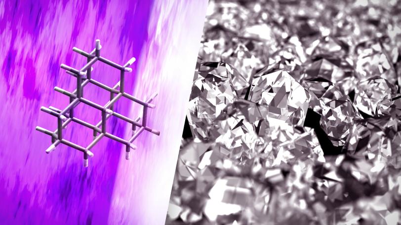
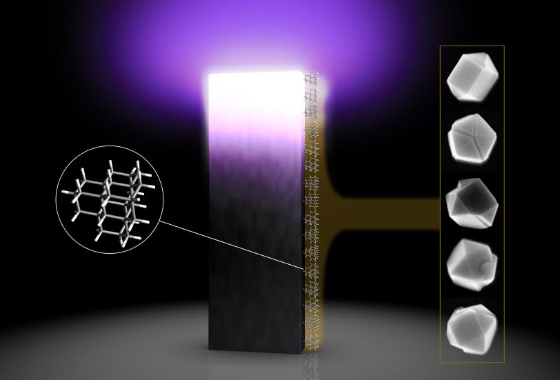
To see how it works at the smallest scale, Melosh and his team turned to diamondoids, the tiniest possible bits of diamond. The smallest ones contain just 10 carbon atoms. These specks are the focus of a DOE-funded program at SLAC and Stanford where naturally occurring diamondoids are isolated from petroleum fluids, sorted by size and shape and studied. Recent experiments suggest they could be used as Lego-like blocks for assembling nanowires or “molecular anvils” for triggering chemical reactions, among other things.
The latest round of experiments was led by Stanford postdoctoral researcher Matthew Gebbie. He’s interested in the chemistry of interfaces – places where one phase of matter encounters another, for instance the boundary between air and water. It turns out that interfaces are incredibly important in growing diamonds with a process called CVD, or chemical vapor deposition, that’s widely used to make synthetic diamond for industry and jewelry.
“What I’m excited about is understanding how size and shape and molecular structure influence the properties of materials that are important for emerging technologies,” Gebbie says. “That includes nanoscale diamonds for use in sensors and in quantum computing. We need to make them reliably and with consistently high quality.”
Diamond or pencil lead?
To grow diamond in the lab with CVD, tiny bits of crushed diamond are seeded onto a surface and exposed to a plasma – a cloud of gas heated to such high temperatures that electrons are stripped away from their atoms. The plasma contains hydrogen and carbon, the two elements needed to form a diamond.
This plasma can either dissolve the seeds or make them grow, Gebbie says, and the competition between the two determines whether bigger crystals form. Since there are many ways to pack carbon atoms into a solid, it all has to be done under just the right conditions; otherwise you can end up with graphite, commonly known as pencil lead, instead of the sparkly stuff you were after.
Diamondoid seeds give scientists a much finer level of control over this process. Although they’re too small to see directly, even with the most powerful microscopes, they can be precisely sorted according to the number of carbon atoms they contain and then chemically attached to the surface of a silicon wafer so they’re pinned in place while being exposed to plasma. The crystals that grow around the seeds eventually get big enough to count under a microscope, and that’s what the researchers did.
The magic number is 26
Although diamondoids had been used to seed the growth of diamonds before, these were the first experiments to test the effects of using seeds of various sizes. The team discovered that crystal growth really took off with seeds that contain at least 26 carbon atoms.
Even more important, Gebbie says, they were able to directly measure the energy barrier that diamondoid particles have to overcome in order to grow into crystals.
“It was thought that this barrier must be like a gigantic mountain that the carbon atoms should not be able to cross – and, in fact, for decades there’s been an open question of why we could even make diamonds in the first place,” he says. “What we found was more like a mild hill.”
Gebbie adds, “This is really fundamental research, but at the end of the day, what we’re really excited about and driving for is a predictable and reliable way to make diamond nanomaterials. Now that we’ve developed the underlying scientific knowledge needed to do that, we’ll be looking for ways to put these diamond nanomaterials to practical use.”
This research took place at SIMES, the Stanford Institute for Materials and Energy Sciences, with major funding from the DOE Office of Science. In addition to SLAC and Stanford, researchers contributing to this study came from the Institute of Physics of the Czech Academy of Sciences, University Hasselt in Belgium and the Institute of Organic Chemistry at Justus-Liebig University in Germany.
Citation: Matthew Gebbie et al., Proceedings of the National Academy of Sciences, 1 August 2018 (10.1073/pnas.1803654115)
For questions or comments, contact the SLAC Office of Communications at communications@slac.stanford.edu.
SLAC is a multi-program laboratory exploring frontier questions in photon science, astrophysics, particle physics and accelerator research. Located in Menlo Park, Calif., SLAC is operated by Stanford University for the U.S. Department of Energy's Office of Science.
SLAC National Accelerator Laboratory is supported by the Office of Science of the U.S. Department of Energy. The Office of Science is the single largest supporter of basic research in the physical sciences in the United States, and is working to address some of the most pressing challenges of our time.