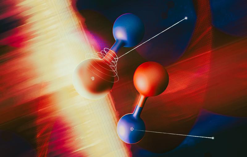
so hello
actually it's not even me you should be applauding i'm just giving the introduction
so i'd like to welcome you all to the slack public lectures this installment will be about the
material world it'll be given by rob moore who is
one of our staff members here rob got his undergraduate degree in mechanical engineering from tennessee
tech then he went into the navy and spent two years in a submarine
and from that experience whatever it does to you decided to go into physics
he has his phd from the university of tennessee and he came here in 2006 to
work at our x-ray laboratory now he's the assistant director of symes
which is the slack stanford laboratory for materials research and
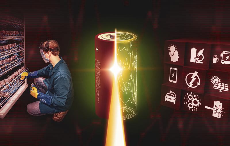
energy research and he's going to tell you about the future of materials
so let me introduce rob and uh
all right thank you thank you oh my public i love it so um
i'd like to thank you for the introduction and you know it's a thrill to be here and it's it's it's gonna be a lot of fun talking about some of our
latest research and some of the things that we're doing here at the lab now there there is one thing though you
know i i would also like to thank sly communications for hosting the event and they also made our nice wonderful poster
here now but i i do have to you know wonder you know with the materials theme and
the material world and and and all of the fashions you know i just wanted to to make
sure you're aware that you know we're not bringing back the 80s that's not where we're going okay so you
know i find i kind of feel like we should have a disclaimer down here so just to make sure it's it's not going to be the 80s
but you know i did actually request sort of a a poster with a fashion theme because my daughter's actually here
watching me tonight and um so that means that i'm actually competing with her cell phone and the gains on us so i'm
trying to have something that sort of appeals to her fashion sets so we'll see how i pull it off we'll see
how it works so now when you think of a material world what what what images come to your
mind i mean do you think about madonna being a material girl in a material world
all of the fashions and all of the trends and latest gadgets and all of the stuff
that we fill our lives with or do you envision some sort of world to where the boundary between technology
and human existence is becoming so narrow that it's blurred as we you know go through and scour
under every other rock around the earth trying to find that last ultimate material unobtainium
so you know these are pretty extreme examples but you know but we can't think about for a second what is the boundary
between technology and our lives and so how far away are you from a
technological device so think about even when you're sleeping i mean you may have a cell phone on your
nightstand maybe your alarm clock what about a pacemaker
and so it comes down to it that technology is everywhere and everything that you see comes down to being built
out of something that was made from superconductors i mean not superconductors but semiconductors
and so you know it's so that's what we'll be talking about tonight and so for me you know i like to know how
things work and so that's the physics background but i also like to build things i like to build things that
can make an impact on the world around us and so that's the engineering background
and so you know when i go to dinner parties people often ask me well what is it i do and you know it's kind of hard to
explain you know within the the few minutes that are typically allowed for a casual conversation at a dinner party
but you know now you know i have your attention for an hour and i've got slides
so um so yeah this is what we do all right so this will be fun so
so there's basically two sides to my job one of them is making materials
and then the other one is actually looking at the electronic structure of the materials by shining light on it
now this seems rather straightforward right but but let's dig just a little bit deeper
but i want to start with just a very brief history to kind of give us sort of a perspective
of where we're going and and what materials mean to our lives
so about 3.3 million years ago are the first historical records of rudimentary
tools made out of stone now stonehenge was made around 3000 bc
and so what does this mean so it takes about 3.3 million years for us to go
from very rudimentary simple objects to being masters of stone from rudimentary
to ornate about 3.3 million years to become masters of all things stone
but then about 6000 bc we learn how to smelt copper extract
copper metal from you know oral that we find in shallow mines and such
and so then about 3000 bc we actually learn how to take copper and mix it with
tin to form bronze now bronze has an age made you know named after it simply because you know
bronze is a strong enough material to where you can make very you know useful farming implements hunting tools weapons
for defense and so you know that that's what really gives it its age
and so that was about 3000 bc and then we come up to about 1200 bc to where we can actually learn how to start
working with iron we developed the technologies to hot work iron control the carbon content
and so this is a situation to where we can get to the point to where we can make just about anything that we want
out of metals and so while this spans several different ages this takes about 5 000
years from rudimentary to becoming masters of every all things metal
five thousand years now the end of the iron age is is you know
was with the development of writing as we go from pre-history to history
but from our perspective as we actually start looking at the journey of different materials and and how they impact our lives
then we need to come to semiconductors and so semiconductors the the very first idea of a transistor
started to appear in the 1930s and semiconductors really started to have some sort of practical applications in
radar technologies in the 40s so but it wasn't until 1947 when the
very first transistor actually became a reality and so from that we actually go from 47
in the mid 70s we actually start having a lot of computer technology and then in the mid 80s we start having the internet
the propagation of all of these internet service providers and the birth of the information age
and so semiconductors from the very first devices made out of just a chunk of a semiconductor all the way
to masters of all things semiconductor about 60 years so to get an idea of today's materials
and sort of the development cycle for today's materials let's talk about something that we call giant magneto
resistance now this is a material property to where you actually can
change the resistance of a material by small changes in a magnetic field
now this is one of the key technologies that allowed us to shrink hard drives down to write smaller and smaller bits and to
read smaller and smaller bits in magnetic media and so we go for about 10 years in 1997
as the first hard drives with the gmr head and then in 2006 we actually start
having micro drives small enough that we can fit in you know pocket held devices
now i really like this picture because it's cute but i pulled it off the web several
years ago and so by now the chicken has already flown the coop and i'm not talking about the chicken
so this is a situation to where now today we actually have solid state hard drives that far exceed the capacity
of a lot of these these magnetic media but it's based on a completely different material technology
but this is sort of where we are today now to gain some perspective
does everybody remember these raise your hand if you know what this is wow yeah all right maybe this is going
to be the 80s night all right i love it so floppy disks
so these were all the rage back in the 80s and so the floppy disk if we actually think about well how much
information can we store here compared to the floppy disks and well
it's about 750 000. now if we actually stack all of these
floppy disks up here on the stage it would fill a box that's about 10 feet wide 10 feet long and 12 feet high
but what's even more interesting is the simple fact that that box of information
would weigh more than eight toyota camrys it's hard to believe that our
information weighs that much
so as we look at this brief evolution of materials and how it impacts our lives there's two things that i really want
you to take home one of them is that the time between materials
discovery and becoming masters and implement implementing that material that time is shrinking exponentially
now the other thing that i'd really like to point out is the fact that fashions have dramatically changed along with the
materials and the technologies so i mean i would really i feel sorry for the person who had to wear this hat
i mean that had to be uncomfortable and the shirt you know that's a great looking shirt but i just don't see me
being able to pull that off i just don't think i could do it
so as we go through the history and we come up to today
and so as we look at today what are we in the state of the art now there are a number of different materials that are
emerging in different technological markets today you have electronic devices flexible
devices sensors batteries wearable devices smart building materials
and so a whole vast array of different materials that are coming on the market and making the dramatic impact on our
world and today i'm actually going to talk about three of these one of them is in the opto electronics
industry to where you can think about coupling light and all the information that you can carry with light think of
fiber optics and how we couple that with our electronic devices the other one is is regarding smart
windows these are windows that can change the transparency to with the flip of a switch in order to help save energy
and last is actually trying to look at superconductors and so trying to figure out how to make better
materials better wire better you know transport energy transport materials and
so if we can actually find a superconductor we could save the world trillions of dollars of wasted energy
just due to the resistance that are in the wires today but the next generation the next age
is going to be down at the level of atoms and electrons and so when you get down to this level there's actually many
more exotic properties that are out there we have superconductivity but we also have things like topological
insulators multi-feroics thermoelectrics photovoltaics
photonics spentronics catalysis there are a lot of very exotic interesting
properties that happen at the level of atoms and electrons and the key is is how can we capture those properties and
make useful devices and interesting things out of them but to start to do that we have to understand them on the
most fundamental of levels so how do we actually make these
materials and how do we design you know look at these exotic properties so here at slack we've actually
developed a program that is dedicated to the investigation of fundamental material
properties that actually generate and responsible for all of the exotic
properties that we see that are not only interesting from a fundamental perspective but could actually be useful for something we
could do something with now this is a program that is actually a collaboration between two different
divisions or a user facility in the the materials science division here at slack
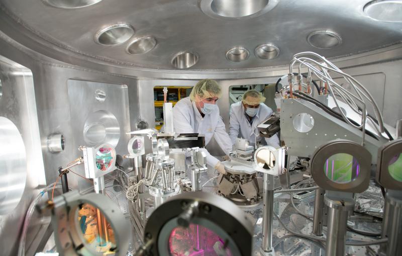
and so this collaboration we have symes the material science division at slack which is actually looking at the growth
of these materials and then ssrl the user facilities to where we can actually map out the electronic structure
and so some of the people in the audience you might actually recognize this instrument here because it was one of the instruments on the recent global
physics photo walk and so this is a photo walk to where amateur and professional photographers tour the different labs and take
pictures of certain instruments and so one of our instruments was the highlight but it didn't win
i know i'm just gonna have to get over that because i mean we have by far the prettiest instrument here at slack i
mean but anyway i'm just gonna have to get over that and so slack is a department of energy
national lab and of course this program is funded also by the department of energy this is
your national lab this is what we are doing for you
so let's dig a little deeper and let's have some fun so let's see if we can understand how materials work on the level of atoms and
electrons let's start with the atom so in the atom you have a nucleus that's
formed of protons and neutrons and protons are positively charged and electrons are negatively charged that
actually orbit around the nucleus and you can see that the electrons are much much lighter than
the protons even though the charge is of the same magnitude
now these electrons take on different energy levels inside the atom and so you know the the higher the orbit
the higher the energy the you know the more energy the electron has as it whizzes around the nucleus but in
addition to that we normally think about you know an electron when it orbits you know the
nucleus we often think about you know an analogy with the the planets orbiting the sun
or the moon orbiting earth but here the electrons actually have
very strange shaped orbits and the higher the energy level you go the more different types of orbits you
can actually find the electron in
so for now let's just think about the simplest of these orbits the s orbital which is just a spherical cloud of
charge if you will now think about this as as a cloud simply because um if you ask well where
is the electron well then you can find it say it's right there but if you don't ask where's the
electron well you'll never know because it's at all places in the cloud at all times
now i know that sounds kind of strange but that's just quantum mechanics for you and so you know i i know it's weird but
you know i i'm sure there's a lot of cat lovers in the audience and so i'm not going to go into detail about what schrodinger
proposed to do to his poor cats you know in a thought experiment trying to explain the quantum phenomena
so we'll just think of this as clouds for now and so if you actually have several atoms together with these overlapping
clouds and you you know this electron right there if you found one right there which atom does it belong to
it's hard to tell what about here you just don't know
you can't tell and the electron can't tell and so if you find an electron here then
you know you can't tell what atom it is and so it's just a basically a cloud of charge that has these periodic array of
atoms inside and so in these conditions the electron is just free to move throughout the
material just wherever it wants to go but now what about here
so in this situation you know if you find an electron right there well it belongs to that atom but if you find one
in here well it's hard to tell but these are different you know these are representing the p orbitals and so the
different orbitals have different sizes different shapes and different overlaps and so in this particular condition if
you have an electron here it kind of hops one atom to the next
now you can tell that it would be easier to hop in one direction than the other
and so the orbits actually play an important role in determining how the electronic structure works how the
electrons actually move through the material so we start making materials we can start taking our atoms
and then we start taking all these different kinds of atoms and start moving them next to each other and you have all of these overlapping energy
levels and what we end up with is something that we call an energy band
now when you think of an energy band think of it in terms of like a road map
and so what this does is it's energy band in momentum and in energy so you know an electron right there it's
basically saying that it's moving in a particular direction with a particular mass and a particular speed
through the material and it takes that much energy for that to happen for that electron to
do that and so just think of the energy bands as a road map if you will
now the shape of this inner the the shape of these electron these energy bands are actually determined by the
types of atoms we have in our material and the locations of the atoms this is what kind of generates the shape of these energy bands
so now we have all of these energy bands we have all of these electronic states but each atom only has a certain number of
electrons in it and so there's always going to be some you know empty states that are of the
same energy and our little example here you know the p orbitals can hold up to six electrons but there's only one right
up here so there's a bunch of extra states in which you could put electrons
and they would be at the same energy as this and so what this means in our materials
while you can think of this as a road map it's kind of a strange road map and the fact that if you add another
electron you know exactly where it's going to go it's going to go to the lowest energy state that's not occupied
by some other electron and so it's a strange road map but it always fills up from the bottom up up to
the maximum level and the electrons that have the maximum energy at the very top we
call this the fermi level or the fermi energy
now i show here also the fact that you know the electrons have spin to it you can kind of see in you know the arrows
pointing up and arrows pointing down now spin think of it as you know the magnetic moment of the electron
and so if you have a material to where you have electrons that are on all of the atoms then they're all pointing in
the same direction you're going to generate a net magnetic moment and this is a magnet just like on your
refrigerator however if you actually have them to where they're pointed the opposite way
then this is an anti-ferromagnetic and so these spins actually determine the magnetic properties of the material
itself so
when we actually have these energy bands and we actually have the fermi level that cuts through one of these energy
bands so that you have unoccupied states just right above the occupied states
then you have a situation to where the electrons can actually use these little unoccupied states to kind of hop through or freely move through the materials
and so in these particular cases these are metals if you have a situation to where the
fermi level is actually between these two energy bands to where you have all of this band here which is occupied but
this band which is completely empty then you're going to have to have a certain amount of energy to kind of jump
the gap and to go from one road to another road and so we call this a band gap
and in this situation none of the electrons can move because there's no free states for them to move in
and so this is an insulator and so the filled states we call it the valence band up here to where if you
could put electrons up there they would move around we call this the conduction band now if the gap is small enough
to where if you have just a little bit of heat or just add a few extra electrons in it then it's going to start
to conduct electricity then this is what we call a semiconductor
now we've been talking about some toy models here and it's it's fairly you know um
simple to go you know with the toy models but as you start looking at real materials things get really complicated
really quick and so this is actually a theoretical calculation of the band structure of the
road maps of a particular material and showing the energies and the momentums of of the electrons as they go
in different directions in different momenta through the material so things can get pretty complicated
really quick now we talked about heat and how it can sometimes add energy to
electrons so what is this so we have what we know is is is phonons
now think of the lattice as an array of just balls connected with springs
and so what happens if you just whack that array of atoms right there what's going to happen well you're going to
have this wave that just starts propagating through this chain of atoms and springs
and so all of these different ways the atoms can move all of these different waves that propagate through these are
different phonon modes and so this is how the lattice can actually transmit energy through the
system now for more complicated materials to where you actually have a lot more complicated structures inside
the materials then the phonons are going to be even stranger and more complicated as you
actually have sort of a all these different atoms moving in concert together representing these
different phonon modes so phonons are how sound propagates through material and it's how heat
propagates through material oh there so
what types of players do we have so we have the band structure and the band structure is determined by the position
of the atoms and the types of atoms that are in our material and then we have all of these players that actually influence the electron the charge of the electron
the spin which orbital it is it is in and all of this lattice energy all of these things
can influence how the electron behaves but there's one other player and i already gave you a hint of it there's
one there's one other player which we haven't talked about yet which is critical to our story here
and that is light and so electrons can absorb light
and electrons can emit light so now that we know the players
what is the game so the idea is we talk about being able to look at materials and control
materials on the atomic level with atomic precision so how do we do that and so we do that by using a technique
called molecular beam epitaxy and so molecular beam epitaxy just think of boiling boiling water in a pot
so as you heat the water up you start to form steam and steam comes out the spout
so what we do is we have something similar to this we have little small pots where we put really pure
materials inside then we stick these pots inside of a chamber and pump out all of the air
and then we just heat up the pots of different materials and outcomes are atoms
and so we shine these atoms on some sort of crystalline substrate some of these things come on and just bounce off and
absorb and some of them hit the surface and they'll start rattling around until they find an ideal crystalline position to
where they can have a chemical reaction to form the new material that we're trying to form
and so in this way we can actually start with the substrate and start growing materials layer by layer by layer
now the neat thing about this technique is the fact that we can stack up atoms in so many different configurations
and you know so it's um and so we can you know start looking at
you know how to control all of these properties and we can actually make things that you're just never going to find in nature
and so that's the beauty with this technique but now one of the things that we need to do
is to understand you know the electronic structure of these materials now this is a very well established technique a lot
of the semiconductors and a lot of the technology that we know today you know has roots in a lot of these
thin film techniques and molecular beam epitaxy is one of them but there's a caveat as we normally can't look at a
lot of the materials created by mbe we can't directly look at the electronic structure
and it's not because of a material problem it's actually because of the electron itself and so when we're
trying to look at the behavior of the electrons the electrons of the material if they come out if you actually take the material out and take it out into
atmosphere then all of the atmospheric contaminants moisture co2 co hydrocarbons anything that's
going to sit on the surface it may not affect the material but it's going to destroy the signal that we're trying to measure
and so that's the trick is how do we get around that
so let's look at the flip side of our program how do we actually look at the electronic structure
and so with the synchrotron at ssrl so we take a long chain of
electrons let's say about a meter long and then we accelerate these two really close to the
speed of light now from our perspective sitting in the laboratory this whole chain of atoms
gets shrunk to just a fraction of its original size and this is relativity
and so as we whizz the these bunches of electrons around the ring in certain
sections of the ring we pass them through a series of magnets that are you know oriented opposite of each other
and so what this does is the magnetic field actually interacts with the electrons and they start to
oscillate as they move through the undulator now remember i said that you know
electrons can actually emit light as it turns out whenever you accelerate charge it radiates light
and so we use that simple fact by having these high energy electrons go through our undulators and by
controlling how they oscillate we can actually generate high intensity x-ray beams
with specific energies and then we just take these beams of light and then
shine it onto our sample now as we shine it onto our sample
that you know the the photon can come in which is just a quantum of light
and it can actually you know couple with the electron the electron absorbs the energy and it can jump to a higher
energy state now the caveat is is the phone is the the the quantum of
light or the photon and absorb is actually equal to the difference between those two energy levels
now the opposite can happen if you have an atom that has an electron in an excited state
as it decays back down to that ground state the state of lowest energy it can
emit photons as it actually jumps from energy level to energy level and so the game that we play is we
actually shine the x-rays onto our sample and we actually look at how much
of the the photons are absorbed and we actually can look at you know how much of the photons are actually emitted
afterwards and what this does is it tells us about the electronic structure and hello
okay all right don't go to sleep now all right
okay uh all right intermission i guess right okay so um
and so what we do is we can actually collect you know the photons coming out and we can look at how much of the x-rays are actually absorbed and it
tells us about the electronic structure the energy spacing between the different levels of the atoms inside the material
now there's a lot of different flavors of this technique and the ones we're talking about today one of them is called x-ray photoelectron spectroscopy
this is basically where we take a photon it excites an electron to an excited state but this electron has so much
energy it just leaves the material and as it leaves the material we actually collect it and resolve how much energy
it had below the fermi level and so you can see it it has very distinct fingerprints and these are
distinct spectroscopic signatures of the materials that we're looking at and then x-ray absorption spectroscopy
we actually sweep the uh the energy of the incoming light and look at how much of the energy is actually absorbed and
this is another way in which we can actually look at the electronic structure and the spacing between the actual energy states and the positions
of the atoms inside the material there's one other technique that we'll
be talking about angle resolve photoemission spectroscopy now this is a situation to where we
shine our light on the material the electrons have so much energy that they just fly out of the material and then we
pass those electrons through our detector and actually map them onto a two-dimensional sort of ccd camera if
you will and so on our ccd camera we have one axis that's energy and then the other
axis is momentum now we can stack all of these plots together to generate a multi-dimensional
representation of the electronic structure inside the material itself
now if you actually look at it here up at the the fermi level here if you actually look at the multi-dimensional
map of the fermi level these are all the states and we call this the fermi surface this is the the all of the electronic uh
states that are at the maximum energy in the multi-dimensional space it becomes a surface and so this
is a a fermi surface
now we know that the players are very limited the number of players
that actually interact with the electron are very limited but we do need to think about a bit of perspective here
and so in order to get some perspective let's think about a one centimeter cube
of stuff you know just one centimeter or just some other little shape that you want to
actually think about that's one centimeter cube and then ask yourself you know well how many atoms are in here
that's a lot of atoms now for metals you're going to have a very similar number of electrons
in there as well free electrons able to move around but
now electrons are all negatively charged and they repel each other very dramatically
and so if you have all of these electrons in there that are repelling each other and squeezing them into the space it doesn't take too much in
intuition to to realize that strange things are going to happen
and so if we want to actually think about what is going to happen we have all of these
different interacting particles and this is what we call mini body fixes because there's so many of them
but now out of this you can actually get collective modes you can actually get sort of of
you know uniform behavior for all the individuals now and since this is you know 80s night
you know in order to try to understand this concept you know i thought i'd help you know bring someone in to help explain what this concept is and what do
you mean by collective excitations and collective modes and so you know without further ado you
know i would like to introduce our guest speaker and so ladies and gentlemen please welcome madonna
i'm sorry is this on hello uh guys in the control booth did madonna
not get our invitation no no oh okay um so well i guess she's not going to be
here tonight but nonetheless you know she still helped us explain what it meant by collective behavior
because as soon as i said her name everybody's eyes went to the door and so just a very small amount of
interaction we can have a room full of individuals that all did the exact same thing
this is what we mean by collective behavior now out of this collective behavior you can actually have a lot of
emergent properties that form in the material and these emergent properties is what generates a lot of the exotic
things that we see in the material physics and we want to learn how to understand them and be able to control
them so in our materials
we actually look at the electrons coming out but are protected detectors are so sensitive enough that we not only look
at the energy and the momentum electron coming out but we can have indications fingerprints of how all of
these different parameters affect the electronic structure
how it affects the behavior of the electrons inside the material and so these are the emergent phenomena
the collective information and the collective modes that we're actually looking at in the materials and and what does this look like
so this this has very different shapes and fingerprints and such in our our data you can appear as band gaps
you can look at band kinks you can have shifts of spectral intensity you can have folded bands you can have split
bands you can have replica bands and all of these things are indications of the different players that are influencing
the behavior of the electrons to generate these exotic properties that we see
and so at ssrl we take the latest and greatest rpes synchrotron we shine the light down it and and shine it on of our
samples and this is how we actually map out the electronic structure of the materials itself
but now in order to look at a lot of the thin films that we're growing via molecular beam epitaxy
we combine these two techniques together and so this is a massive system but we actually have growth systems here to
where we can develop different films and then we move them just straight into our rpes system to where we can map out in
very precise detail the electronic structure of the materials
and so with that i'd like to take um some time to actually look at some of
our results so now that we've seen what the electronic structure is and how can we measurement what does this mean what are some things
we can do with it so the first little story here is is something that you know i'd like to talk about
smarter than you think windows and so what this is these are
electrochromic nano composite nickel oxide materials i tried to say that one 10 times in a
row really fast i'd like to see that so what these are is these are basically
these are materials that that'll change color when you apply a voltage and so the idea is you can coat them on windows
and so um and this is something to where you know if it's a hot day you can flip a switch it blocks the sun and it's nice
and cool inside so these are are you know used for smart buildings
in order to help save energy now the material the material study in this particular case was lithium nickel
tungsten oxide and this is a collaboration with the national renewable energy laboratory to where
they actually made the materials and then we investigated them at ssrl
and just to give you a scale that the actual material is right here the little color green and it's about 80 nanometers
thick so this is the x-ray spectrum that we actually got from the materials now you
can kind of see that that you know the top curves look kind of like each other the bottom curves are pretty close to
each other but comparing the two they're just completely different and the same with our xps spectrum it
just looks like different materials and so with this it this actually reminds me
of um one of my favorite science quotes and it's actually by a a a
scientific or a science fiction writer and the quote is you know the most exciting phrase to hear in science the
one that heralds new discoveries is not eureka but that's funny
now this was kind of weird we weren't expecting this but now what's even more weird is this
peak right here i mean that's just strange why is that there that just doesn't make any sense what is that
and so the what it turns out is the techniques the techniques that we were using are very surface sensitive xps and
if you look at the total electron yield of x-ray absorption spectroscopy is very surface sensitive
and so as we would start to cycle these materials start to add charge take charge out then it actually started to
form lithium peroxide on the surface and this peak here is a very unique fingerprint for lithium peroxide it
can't be anything else and so what this is telling us is we actually start looking at sort of a
charged and discharge state or a transparent and opaque state
then we're starting to form this lithium peroxide on the surface and so what happens then the lithium comes from inside the
material to form lithium peroxide on the surface and then as we start to discharge it the
the um or charge it back i guess the lithium peroxide dissolves and the lithium goes back into the material
and so what this does is it actually shifts the amount of charge inside the material which actually you know
generates some extra states inside the material that allows the absorption of
light so we learned from a very fundamental level what makes it change color and why
but also what's interesting about this particular case is the fact that the the movement of charge the movement of
lithium ions into and out of material in the formation of lithium peroxide this is exactly like a lithium-air
battery and so what we're saying is we have an auto tinting window that acts like a
battery you shine the light on it it changes how many electrons like to hang out on the
nickel changing the number of states available for the absorption of light
but also it's it's acting just like a solid-state lithium-air battery
so let's take just a second and kind of go from the world to science into science fiction and what does this mean
so let's envision we have a small building or a house that has lots of glass on it
and let's put solar cells on top of the building so as the sun comes up the solar cells
will start to generate energy and it gets the hot part of the day your solar cells will generate so much energy
that you don't know where to put it where you're going to stick it stick it in your windows
so as the sun goes up the heat comes in you store the charge in the windows to
help minimize how much heat is getting inside the building and then as the sun goes down and your solar cells are
starting to generate less charge you can just pull the charge out of the windows and they become clear again in the
evening now this is pure science fiction this doesn't exist and a lot of it is probably because capacities there's only
going to be so much charge you can store in windows and you know buildings require a lot of energy to operate
but nonetheless this is something to wear a lot of the latest battery storage technologies these this type of scenario
is on the horizon but it's going to be much better than this
so let's take a look at our next little example but now for this one we have to take a short quiz
yeah i know you gotta love it right so what are these things should i start asking questions and point to people
so remember our energy bands so we have our energy bands you know occupied unoccupied states
now the way that we draw this is necessarily so i mean there's no reason that these things have to be lined up
with each other and so if we have a situation like this
and you know we shine a photon on this well then we can actually excite an electron into this energy
level and the reason for this is because the photon has negligible momentum
compared to the electron and so it can generate these atomic transitions these energy band
transitions but it can't change direction which means this has to be a straight line up and down
and so on this side we can actually generate a transition but you require a much more energetic photon one with much
shorter wavelength much more energy to reach from this state all the way up to there
and so is is there no way if we say we only have this wavelength of photons is
there no way we can actually get over to those states it turns out there is
and this is how we can start thinking about electron phonon coupling how the electrons and all these lattice vibrations
coupled together now one way to think about electron phonon coupling is to actually start
with the hamiltonian and then you know let's not think about it this way
let's think about it this way oh yeah let's think about the physics of the
alley-oop
and that cool i don't care who you are these guys are impressive it just it's awesome
so if you think about the the idea of an alley oop you have one player that just lobs the ball up somewhere close to the
goal and then you have another player comes over and just finishes the job so let's
think about this in perspective of electrons so let's just think of the basketball is our electron
and so you know one player it goes up you know it has the energy to make it it
has the distance but all of a sudden a phonon comes by and just makes it change direction and goes into the state that
we want right through the basket and so this is sort of what we mean by
electron phonon coupling so we have a situation a photon comes in it starts to excite an electron but then
all of a sudden a phonon comes by and just gives it a push of momentum to actually make it over into the state
and so now this is possible however it takes a really concerted effort of the phonons the
lattice the electron the light and so it's possible but it's just a very low probability of it actually
happening that way not when it is compared to something like this
now in our sort of loose basketball analogy here you know a direct band gap transition
is something to where you can envision yourself right above the basketball goal now i
cannot play basketball but i could probably make that shot
and i could probably make it most of the time and so this is a situation to where you
know you don't need any change of direction it's just a straight energy shift without changing the direction of
the electron now the neat thing about quantum mechanics is this is actually backwards
the scenario that we're actually talking about you would have to envision the basketball setting on the floor all of a sudden getting light absorbed a photon
and it just jumps up through the hoop right into your hands that's the cool thing about quantum mechanics because this is how energy is
exchanged on the quantum mechanical level and so this is a direct band gap transition and if it's over to the side
we call that an indirect band gap transition and so for these next materials
transition metal dicalcogenides and so these are materials that are very interesting because
if you look at a material that's just one layer thick then you have this very large non-linear
response to light now this is pl means photoluminescence so this is basically a technique to where you absorb you know
you shine light on a particular wavelength it the electronic sights up and then it comes right back down for
that energy it's just a straight direct transition and so you can see for one layer you have this very large response to the
light but if you grow it two layers thick or thicker nothing happens
it just doesn't you know the light just doesn't do anything to it now theory has suggested that this is
actually responsible this is actually due to a transition from an indirect to a direct band gap as you shrink down
this material to one layer thick and so if we actually so we grew some of
these materials and if we actually look at some of our data now this is eight layers of molybdenum disillinide
and so here is our rpes spectrum now one of the tricks that we do in order to understand because here you
have a situation where here's the valence band maximum but you don't see anything up here because our fermi level
is inside that gap now one of the tricks that we do is we take just a little bit of potassium and
sprinkle it on the surface now potassium is an alkali metal and so it has one electron in its outermost
shell and it doesn't like to be there so as soon as you put the the alkali metal on the surface the electron jumps
off and actually goes into the material so we're actually shifting
the position of the fermi level due to adding this potassium and so when we do this and take a look at our
spectrum then all of a sudden you can see the bottom of this conduction band right
there up at the fermi level but now you can see that yeah these are not lined up with each other this is an
indirect band gap but now as we actually shrink this thing
down to one layer and do the same trick where we add potassium on it then all of a sudden you
can see this is a straight shot from the valence band maximum to the minimum of the conduction band
and you can see what happens is just the shape of these bands actually change as you shrink down to one single layer one
single unit cell of the material but now something else i want to point
out is the fact that you see the little blue arrow and a little red arrow here that's because
this band the spins of one orientation and the spins of a different orientation have
different energies and this has to do with the symmetry inside the material but the splitting of
spin states can even be observed inside our spectra
now these and this is interesting not only from just a fundamental materials perspective
this is a situation to where you can actually think about using these types of materials and devices
because we can expand the bandwidth and the efficiency in our opto electronics the coupling of the
information that's inside light and how it interacts with our actual devices
these can actually improve greatly improve on the level of quantum mechanics greatly improve
the efficiencies of these materials and it has to do with just this simple fact you're going to a direct band gap
as you shrink down this material to one layer thick and theory suggests that this could be
an ideal and there's these little transition metal dicatrice there's a whole zoo of these materials
that have similar properties that can be explored but what's even more interesting than just the fact that you have this tunable
direct band gap is the fact that because of the symmetry inside the system
you can think of energy bands at different locations in the material and you can actually couple to different
energy bands depending on the light that you shine on them whether it's right polarized light or left polarized light
you can couple to either wait which all right the red's right all right so you can couple to the red
bands or you can couple to the blue bands now you couple that or you combine that
with the fact that you know our spins in our valence band are at different energies and now all of a sudden you
have different channels to which you can couple to the electronic states in the materials
and so this is very unique in improving not only the efficiency of the transport of the information but also information
storage and allows for things like valetronics and spintronics where you're actually
looking at the different valleys and the different spins of the material and so this is a very rich phase space
for us looking at the next generation of opto-electronic devices and storage and it's all possible with this
direct band gap resistance is futile
super conductivity so our last little topic today is based on superconductors now superconductivity is electrical
current without resistance it's the free flow of electrons and they
don't have any interactions with the lattice that would help you know destroy that energy it's free-flowing without
resistance now superconductivity was discovered back in 1911
and then in 1957 bcs theory came about that kind of
explained how these superconductors work and to think about how a superconductor
works is think about our lattice array here and as the electron is moving through
well then you have this negatively charged electron interacting with these positively charged lattice
and the lattice will start to distort this is that electron phonon coupling if you will
however you know in this scenario think about you know the atoms are moving very slowly to where the electrons are
zipping through there very fast and so as this electron leaves the material then there is going to be a net
positive charge if you will right in this area which is going to attract another electron
and so in this way these electrons actually will start to pair up and can move through
the material without resistance due to the assistance of this phonon this electron phonon coupling
now this is how conventional superconductors work but then in 1986 there was discovery of the cuprates and
what we call high tc high temperature superconductors now these materials the way that they
work yeah i don't know it is still complete mystery today we don't understand from
the most fundamental level how these materials work
although that doesn't mean we can't do useful things with them still nonetheless and so the material that i'm going to be
talking about was actually um discovered in 2012 by a Chinese group and it's basically these iron selenide films now
it says films but basically bulk iron selenite thicker materials a
chunk of iron solenoid is indeed a superconductor but the problem is is the fact that its
superconducting transition temperature is really low to where these films if you shrink it
down to a single unit cell it's an order of magnitude larger
in temperature that you actually have these superconducting properties now that's just kind of weird and we
want to understand why that is and how can we take advantage of that
so these iron-based superconductors there's a whole you know zoo of these different superconductors and they have all of
these different crystalline structures but all of the action all of the superconducting properties
lives right inside this iron selenium layer right here and so as we go through the different
materials you can kind of see the the changes in the shape of the fermi surface actually actually start putting
different amounts of electrons on the iron atoms as they move through the material
so this is how we can actually change the shape of the fermi surface and see how it interacts and then you
know changes the properties of the material now arp has on these iron solenoid thin
films angle result photomission spectroscopy so this is some of our data and so you can kind of see that if you
look at just one layer and even two layers of iron selenide i they're different the electronic
structures are just completely different and so that in itself is sort of strange enough as it is
but then you know there was actually something else that kind of appeared that kind of puzzled us a little bit
these little replica bands now these red club commands actually reminds me of one of my favorite science
quotes by a science fiction writer the most exciting phrase to hear in science
the one that heralds new discoveries is not eureka but that's funny
so this is a situation to where this is really it's not supposed to be there and it's never been seen before in
a solid-state material with such clarity and so and these are key are key to what
is going on in these materials and how they behave and so we also did our little trick to
where we can sprinkle some potassium on it to change how many electrons are in the band structure and actually
change the electronic structure and so if we take something just three layers thick to where it looks like a
bulk like electronic structure we sprinkle a little potassium on it and all of a sudden we recover this
electronic structure of that single unit cell that single layer thick film
the difference is there's no replica bands
now the reason i really point that out is because
is because the fact that you know this is itself is actually a superconductor
and it actually has an enhancement of tc but it's just not near as big as that single layer thick film is and so what
are these replica bands we can go back to our our electron phonon coupling here but this is a completely different type
of electron phonon coupling in this case the phonon doesn't come in
and just change the direction of the electron in this particular case
the phonon comes in and just gives a slight kick in energy to the electron
but doesn't change its direction and this is very unique property and
this is what's generating that replica ban that unique signature inside our material
and so what we have is we have bulk materials that have a very low transition temperature for
superconductivity and then we can kind of sprinkle a few electrons on that change the electronic
structure and we have some slight enhancement but then it's coupling
with these phonons inside the substrate that is giving this turbo boost if you
will to the superconducting properties of these materials
now this is sort of of of unique and and you know just you know for the experts in the audience
i'd like to kind of push our little analogy with the soccer ball one step further because remo before when i was
talking about superconductors remember i said that we normally think about the ions moving very slowly while the electrons move very fast
and so typically the electrons are at a much higher energy scale than these very low energy lattice vibrations
but in our particular case in our particular case
the bottom of this band is only about 60 millivolts while the phonon energy is much higher than that
and so this is a scenario to where the phonon energy scale is actually larger than the electron energy scale
and so that's strange in itself and there's concerns about our adiabatic approximation but
my theorist friends tell me not to worry so i'm not going to worry so we have a situation to where we can
actually control the substrate where we actually have coupling between the phonons and the oxides that move across
the interface and actually couple to the electrons that are moving in this two-dimensional material
and it comes down basically for the experts it comes down to screening basically if you have an oxide substrate
here it's where you have these phonons you don't have electrons floating around that can screen
the oscillation of that charge and so that means that it gets really amplified and really connects to these
electrons flowing in this two-dimensional plane now
what's really really interesting about this is there's nothing special about iron selenide
so our theories will show that it's this anisotropy and the coupling in this dielectric
constant that is actually generating this turbo boost for the superconducting properties
so in principle we can actually stack together a lot of different materials and even think about cuprates
and still be able to generate this cross-interface coupling between these different parameters these different
players in our material and so this is sort of the direction that we would like to go
with here with those materials so um
i see that i'm right now out of time and i don't want to be you know any more than fashionably late
so i'd like to go ahead and just you know wrap it up here and so i'm hoping you have a little bit under better
understanding of what this image means and so you know here we actually grow
materials via molecular beam epitaxy and then be able to look at them at the electronic structure
very precisely using the user facilities here at ssrl
now there's one thing that i've kind of you know neglected in this study here and that is theory
so with our theory today and this is one of the things that sets our age apart from
previous ages is the fact that our theory is becoming ever and ever more sophisticated and
we're combining the theory with a lot of the advances in the information age we
have giant supercomputers bigger and better that can calculate more complex systems and our theory is getting better
so that as we calculate those more complex systems the answers are even more accurate
and so what we do is we can actually think about a feedback to where we have a theory that can predict a particular
material we can grow the material and then we can benchmark the theory to see if it's right or not and use this
to do a sort of a rapid materials developments to generate the properties that we're
looking for and so what we're doing is we're actually taking the toolbox the tools
that we have that nature has given us but we're actually generating materials that just don't form in nature
so these are more akin to supernatural materials if you will
so our program offers insights that will define the next age
and with the exponentially shrinking development cycle between discovery materials and implementation
into devices and such this age will happen within our
lifetimes now in a program like this can really
only happen at a national lab to where you can couple the material science division with the actual user facilities here at
the national lab this is your national lab this is your slack and where we're going with it
so now that we're actually here at the end i thought i'd have a few final thoughts about what the future may hold
now i was going to make a joke about you know these futuristic machines that you have in science fiction films
to where you go up to the computer and you ask for a cup of coffee a cheese sandwich and a light bulb and they all
just materialize right in front of you but then i read an article where we're starting to make sports cars with 3d
printed aluminum parts and so i'm not even going to try to make any predictions anymore
but now nature has given us a tremendous toolkit for solving some very tough problems
everything in your life is touched by fundamental materials research in some way
now the rabbit hole is deep there's a lot we don't understand alice has nothing on me or my colleagues
so as this is you know a fascinating world where such few players can actually generate the complexity of
everything we see around us but as we shrink the length scales of
our technology and be able to gain efficiency minimizing cost minimizing carbon footprints
we're going to shrink down to the two dimensional limits now this is where the electronic
structure and the material surfaces and interfaces will dominate the material properties in the physics that we see
and so the fundamental understanding of how the players interact on this level is how we can win the game
and so merging the information age with the material age leading to a materials renaissance and
we are just at the dawn of it and so here is slack we're at the forefront of the wave our mbe arpas
program is now built it is completed you saw the assembly of it and we already have our first data
so let the games begin and with the rapid materials developments that we see within our lifetimes it is going to be a fun ride
but now with regard to what future societies will look like it's going to be hard we
can see the the impact we can make on materials and the positive impact we can make in
everybody's lives but predicting future societies is going to be tricky just as it is with trying to predict
google facebook and twitter would have been the results from the discovery and the development of a semiconductor a
transistor it's hard to say but now there is one thing i do know
about the future and when that next material age happens i do know one thing
i know what i'm going to be wearing because i can totally pull that off
and so with that i would like to thank all of my collaborators who worked tirelessly on all this research and of
course our funding agency the department of energy and with that i would like to thank you
and i'd be happy to take any questions
all right so i guess these are new microphones we're all figuring out how to do it so um yes so
yes we have time for some questions now right now we have these new microphones
we would like you to make sure the microphone is working before you ask your question because
this lecture is being recorded it'll appear on youtube and so we'd like to record your question
as well as the answer what you're supposed to do is to push the button in the middle at the bottom and then the
microphone a red button will appear the microphone will turn on and then you can ask your question and please don't do
that until you're recognized by the speaker so that we don't have multiple people talking at once and we'll start
with this lady right here yes
oh wow okay that works all right okay um my question
is about um photons i was wondering is there a way to measure photons because i
know that they're like uh they're a wave that like propagates through an atom and that uh there's like
the photon push in elements with like electron coupling so can photons be
measured as a as an entity now it actually turns out that photons
can be measured as an entity itself um the the techniques of getting to the
point now to where you can actually start looking at to the point of single photon spectroscopy if you will
now a lot of the detectors and things that we use don't go down to that granularity now we do with the electrons
but not with the photons so our detectors in our pes is detecting one electron at a time
and it cascades into where we can actually generate the image on the detector so there we're actually looking
at single particle physics we're measuring one electron at a time and so while it is possible to actually
measure photons and the techniques that we use we're not going to quite that granularity for looking at electronic
structures thank you sure yes in the back
um so i was wondering like what percentage of time currently do you get
sort of like a that's funny reaction to your work versus oh that did what i expected it to do
like i'm just curious like like are you how often yeah like as your theory improves are you get are you able
to better expect what's going to happen or is it still at the stage where things are completely unpredictable um
well yes or no or actually i guess yes and yes um so this is a situation to where you can kind of see that about two
out of three times something strange happens we don't understand but our theory is becoming much more
sophisticated and much better improved and so with this we can actually you
know start thinking about having theories help us develop materials which is you know sort of what gives us this
this new dawn into the renaissance because our theory is becoming so sophisticated but that being what it is
i'm not worried as an experimentalist you know i i still have job security because we're always going to find
things that just doesn't match the theory that we just don't understand and so it really depends on how deep you
go uh is to there's always going to be something that that you know the theories in the end are models if you
will that helps us understand how the materials behave but there's always going to be properties and there's always going to
be aspects that just pop up that we don't yet understand and so from the very fundamental physics
of electrons and atoms there is still so much we don't know it's a very very deep rabbit hole
but it's nonetheless fascinating to investigate but for a practical sense for the actual
use-inspired materials of actually making things to make devices and useful technologies out of
we're at the point now to where our theory is becoming sophisticated enough that we're having a much more rapid turnaround time for
investigating materials and actually the predictive capabilities of new properties of materials
and so the transition method like dicalcinites was one that was led by theory topological insulators is another
class of material that's really led by a lot of the theoretical efforts and so there's now starting to turn to have
that turning point to where theory can start leading the development of a lot of new materials and this is what's new
we're actually to that point now but that doesn't mean that theory knows at all we're always going to have some cool
surprises that they have to figure out yes
hello
after you're done with your mic and you press the button to turn it off it looks like it's off
me maybe yes thank you oh okay sorry i guess i'll
take your question how about that i'll get yours in a second yes yeah it's like gay
and my question is number one if you can put back the chart with all the
materials it shows the temperature on the side you know how you showed the years versus
the temperature for superconductivity right so most of them are at much lower temperatures than normal room
temperature obviously yes is that one of the limitations
now you know one of the the caveats was super conductivity this one yes yes this
one and so yeah i i kind of glazed over that to not go into any detail but you know these temperatures
are really cold much well below room temperature
and so the ultimate goal the ultimate thing that we would love to do is to be able to design and build a
material that will be a superconductor at room temperature but we are very far away from that
that's the main limitation i would assume that is still we are very we're still very far away from that and a lot
of that has to do with the fact that still that the fundamental mechanism generating the superconductivity
generating the glue that pairs these electrons together so that they can propagate through the material
it's still unknown that's one of the things we can help but the hope here and the new avenue that
we're able to presume pursue now is the fact that with this study is we're starting to find new ways
to actually enhance some of these properties like superconductivity
and so you know for this film you know we can actually look at you know a dramatic superconducting enhancement and
so the idea is can we apply a lot of these techniques and a lot of these ideas to some of these other materials
to get the same similar boost in transition temperature now it may not get all the way up to room temperature
but the hope is that we can eventually get something at a high enough temperature to where we can use it for practical devices
like you know energy transport and transmission lines for electricity
now just to say that even today there are some substations and such that are
have current flowing between them using superconducting wires and so this technology is there today
but because the temperatures are still so low it's not really widespread and so this is where we'd like to be and
this is hopefully a path that will help us boost up getting closer to that ultimate goal
actually i know you let's see if we get the still no work there it is all right you'll not believe it but that was my
question okay thank you all right two questions with one answer excellent
yes that's a pretty interesting machine you have there and is it what's the
throughput and the cycle time between depositing with molecular uh eptaxy
a new material characterizing it generating this arpa's spectrum and then
understanding what that means with decades of education i'm sure
to recognize that something is unusual there and is there hope to automate that process to uh in the same way that in
the huge phase space of genetics and biology nowadays we just do shotgun shotgun approaches to find interesting
things do you have hope for that here and how can i help we'll probably not go that far um now
there is been a lot of of automation in the semiconducting industry for a lot of
these these thin film techniques like molecular beam epitaxy and so even the different versions of
these machines can have robots that move samples in and out and manipulate everything
and so if you actually start trying to think about scaling up a material in order to you know generate some sort of
technological device or something like that then this is a scalable type of technique to where you can do that
because it's it's already been done once but now what we do is we actually look at just the very
fundamental material properties and so we pretty much have to do this at a material at a time
and so for each of our materials it will take a while because you know
the material electronic structure is just so sensitive to the position of the atoms that we have to get really good at
controlling the position of those atoms in a particular material before we actually look at it in our rpes you know
in station and so from that perspective you know it'll take quite a long time to look at
a particular material system and for us to investigate the electronic structure and so for us it's a bit more labor
intensity because it's a material at a time but we're really learning how to control the electronic structure and
once we do that and once we have that knowledge then that could be directly transferable out into industry in order
to generate you know new materials for new devices for example what's the cycle time for one sample
i you know there it's hard to say i mean because it's just for some of our samples you know for uh you know in this
little guy here the couch and i'm looking to be mepitaxi system um it's a looks like a small baby mbe
system so we call it bambi um so in this system to grow a film it takes 30 seconds
and so then it'll take you know maybe a few hours to map out the electronic structure
but now some of the more complicated structures like you know heterostructure is made of titanates and cuprates
you know we're spending months trying to figure out how to get these pieces of the puzzle to fit together precisely
enough before we even stick it into the beam line and take a look at it and so there but once we develop those
recipes and and we've done this with with a lot of different header structures of some tight knits and cuprates
once we develop the recipes it's a matter of growing a material in an hour and then taking a couple hours to
actually look at the electronic structure but that's only after months of developing of the material itself
let's just take two more questions so anyway yes
change of subject the pictures of people working on the gear at the end yes they all had purple
gloves on yes what happens if you don't use the gloves uh we don't get the vacuum we need
so we work under ultra high vacuum conditions and just like i was saying before to where if you actually have a
material any atmospheric contaminants you know moisture carbon dioxide carbon monoxide anything
like that can actually sit on the material it may not affect the material but it will interact with those
electrons as they come out and destroy the signal that we're looking for and so in order to actually do this
technique to have the electrons come out of the material and into the protector we have to pump out all of the air
and we actually have to get to ultra high vacuum conditions on the order of 10 to the minus 11 torr
now i think in the middle of space i think it's 10 to the minus 13 torr
and so it's it's you know incredibly low vacuums no atmosphere whatsoever inside
those chambers now in order for us to actually reach that we have to make sure that we don't have
fingerprints any of our oils as soon as you start pumping it out it just outgasses
and so we have to make sure we keep the insides of these chambers and everything absolutely pristine clean
and after we assemble it we actually wrap this whole thing up and bake it
we actually raises the temperature of this entire system all the way up to 150 degrees celsius or about 300 degrees
fahrenheit just because water is a polar molecule and so it likes to stick to everything
as we actually have to heat these things up to actually get even the water off of the wall so that our pumps can pump it
out in order for us to achieve the vacuum levels that we need and so the purple gloves are just to
make sure that we don't contaminate the inside of the chamber or any of those you know components on the chamber
that would prevent us from actually achieving the vacuum levels that we need in order to actually develop these materials
yes um back to that superconductor chart okay you didn't talk at all about
the thing way up in the upper right corner which looked like it was getting close to room temperature that green dot
in the upper right um that is yeah and the reason for that is
let's see if i can do this real quick we can just take this guy and move it out of the way and you can kind of see that
this is still ah you've got it minus 50. did i really just do that that was 200
kelvin that you saw up there and so it's still you know significantly below room temperature it's it's still
well below and so you know it's something to wear you know it's one of those things that we'd like to achieve but it's something
to where we're going to have to find the tricks in order to actually have this quantum coherence state live at such
high temperatures because a lot of the exotic properties that we see they're easy to appear at very low
temperatures these are the ground state basically the lowest energy level configuration of the materials
themselves but once you start adding heat to it then a lot of times you can scramble a
lot of these quantum mechanical states and so the trick is is how can we actually enhance these quantum
mechanical states and so that they survive at higher temperatures and that how to do that is is the 64 000
question and so by learning how to couple a lot of these different properties together
across interfaces and such like that we can help to try to find ways to enhance these quantum mechanical
properties and so these ground states these exotic properties that we see survive at much higher temperatures that
can be much you know useful for applications and superconductivity is a perfect example of that
so it's going to be a long time before we start having you know superconductors in our cell phones and in our lights and
stuff like that but this is something to where if we could boost the tc up we could start thinking about you know just electricity
transmission over great distances because i think about what is it seven
to ten percent of the total electricity that's made in the world is just wasted
it just floats off into space as heat because as you start moving current through the wires the resistance of the
wire just generates waste heat and it just gets wasted and so if we could find you know a way
to transmit large amounts of current without that resistance the world will forever be a different
place so that's the ultimate goal but we are still quite a ways away from it but
we're starting to understand the players and how they interact with each other to give us hopes of being able to develop
those materials okay let's thank rob again okay thank you
so um rob wants to clean up here but he'll be out in the lobby in just a minute if you have more questions he'll
be out there you can ask him privately the next one of these lectures will be in november
the week before thanksgiving we'll tell you how to discover dark matter with large tanks of liquid xenon
so we hope to see you there and thank you very much for coming tonight