In a first, researchers image the full structure of trapped excitons
It’s a significant step in understanding these whirling quasiparticles and putting them to work in future semiconductor technologies.
By Glennda Chui
Researchers announced today that they have imaged the exciton’s electron and hole to produce the first full picture of this elusive quasiparticle, and showed how excitons can be trapped in dense, stable arrays. The results, they said, have important implications for the development of various future technologies and the quest to understand excitons better.
The study was led by researchers from the Department of Energy’s SLAC National Accelerator Laboratory, Stanford University and the Okinawa Institute for Science and Technology (OIST) in Japan, who published the results today in Nature.
“When light interacts with matter – whether in absorbing light in photovoltaic devices to produce solar power or in creating light from electricity in LEDs – excitons can play an important role,” said SLAC and Stanford Professor Tony Heinz, who led one of the three research groups that collaborated in the study.
“Both for fundamental understanding and for the development of new technologies, such as single photon emitters for quantum information science, we need a comprehensive picture of the nature and properties of excitons.”
Another potential application is information storage, said SLAC staff scientist Ouri Karni: “Excitons absorb and emit light, and they could be used to store information if they were confined to a place that can host only one exciton at a time. This requires them to all be similar to one another and to be confined very nicely, so trapping them is important.”
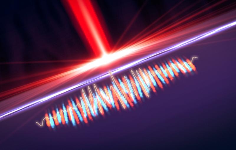
Excitons are created when light hits a thin film of semiconductor material. This kicks electrons out of their usual places in atoms, leaving vacancies called “holes” that move through the material just like electrons do. When an electron and a hole form a brief bond, an exciton is born. The electron and hole twirl around each other like a pair of dancers holding hands, and they travel along that way until the electron falls back into the hole.
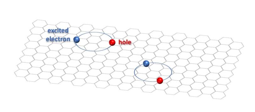
However, the exciton’s short lifespan – as little as a billionth of a second – has slowed the progress of research on them. The longer excitons stay together, the more scientists can learn from them and the more useful they can be.
Peering inside an exciton
Until recently, by far the most common way to study excitons was to see how they absorb, emit or reflect light, said Keshav Dani, an associate professor at OIST who leads the institute’s Femtosecond Spectroscopy Unit. But this approach has significant limitations. For one thing, some excitons are “dark” in the sense that they don’t interact with light, so they can’t be studied that way.
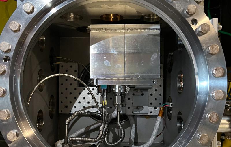
About a dozen years ago, Dani started developing and refining an existing technique called tr-ARPES – time-resolved angle resolved photoemission spectroscopy – to examine excitons and other quantum phenomena in new ways.
“With the instrument we developed,” he said, “we could peer inside the exciton and look at the distribution of both electrons and holes.”
When the instrument was ready to go in 2019, the first thing his group did with it was visualize and measure dark excitons. They were also able to determine the balance and interplay between dark and bright excitons in an atomically thin film of semiconductor material.
Around the same time, Dani started collaborating with Heinz and with Stanford Assistant Professor Felipe da Jornada, whose research groups had also been studying excitons.
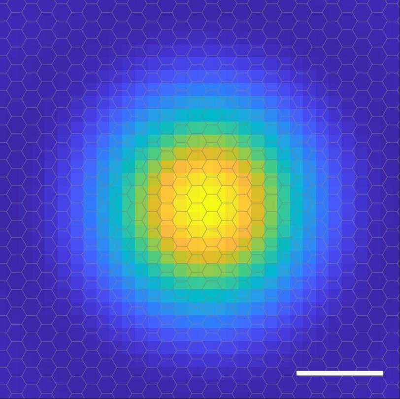
Last year the combined team announced that they had obtained the first image showing how the electron is distributed with respect to the hole in an exciton. “This is like finding out how far apart the dancers are – how far their arms stretch as they twirl – but it doesn’t tell you where they are on the dance floor,” Karni said. “For that, you also need to image the hole.”
Building an exciton trap
In this latest study, the team examined excitons that form at the interface where atomically thin films of two different semiconductors meet. This is an exciting frontier because these excitons can persist a thousand to a million times longer than those in single layers.
First they measured the size of the exciton’s hole for the first time – a real challenge because the hole is the absence of an electron, not a real particle, and it doesn’t emit any signals of its own. The researchers were able to identify the holes by the distinctive gaps they left in the experimental data.
“This allowed us to get a much more complete picture of both the motion of the electron around the hole and the motion of the entire exciton,” said Elyse Barré, who was a graduate student in the Heinz group at the time of the study.
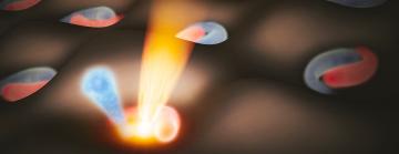
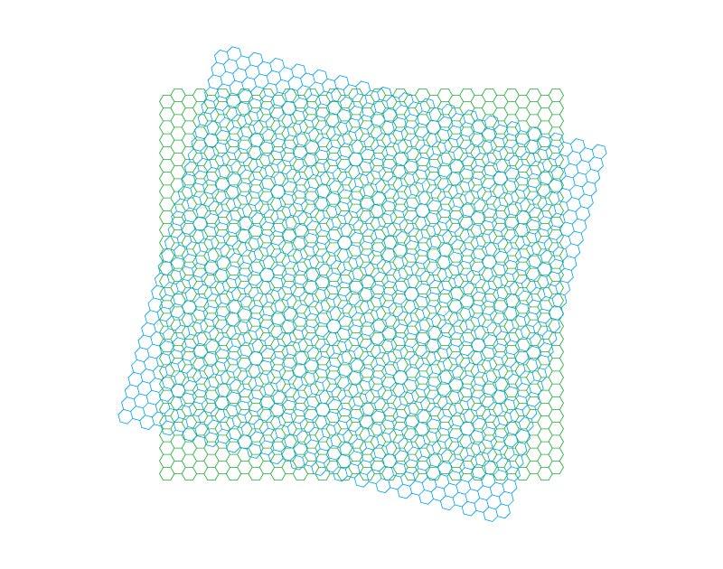
They then set out to trap excitons by layering thin films of two different semiconductors at a slight angle to each other to create a moiré pattern on an atomic scale. (You can make a large-scale version of that yourself by laying one window screen on top of another at a slight angle). Each hole in the moiré pattern is a sort of energy well that can attract and hold a single exciton, and the materials were designed so the wells would be about as big as the excitons, or even slightly smaller.
When they looked at the moiré structures with tr-ARPES to see if and how the excitons fit into it, they discovered that each exciton sat snugly in its well, like a golf ball cupped by a tee. This was unexpected but fortuitous: It was thought that it would take larger wells to capture excitons, but smaller wells are preferred because they’re much more stable and form more uniform arrays.
With this new ability to comprehensively image composite particles such as excitons, the collaborators say they can move forward to explore more complex arrangements of electrons and holes that will shed light on the nature of many-particle interactions in 2D and other quantum materials.
“Our colleagues at OIST have built up very special measurement capabilities,” Barré said, “and we’re lucky to have been able to collaborate with them.”
OIST staff scientist Michael Man, graduate student Vivek Pareek and postdoctoral researcher Chakradhar Sahoo and Stanford graduate student Johnathan Georgaras also played key roles in this work. Materials were supplied by Columbia University and the National Institute for Materials Science in Japan. The SLAC portion of the research was funded by the DOE Office of Science, including theory and computational study through DOE’s Center for Computational Study of Excited State Phenomena in Energy Materials (C2SEPEM). Work at OIST was supported by the Okinawa Institute of Science and Technology, Graduate University and the Japan Society for the Promotion of Science.
Citation: Ouri Karni et al., Nature, 9 March 2022 (10.1038/s41586-021-04360-y)
For questions or comments, contact the SLAC Office of Communications at communications@slac.stanford.edu.
SLAC is a vibrant multiprogram laboratory that explores how the universe works at the biggest, smallest and fastest scales and invents powerful tools used by scientists around the globe. With research spanning particle physics, astrophysics and cosmology, materials, chemistry, bio- and energy sciences and scientific computing, we help solve real-world problems and advance the interests of the nation.
SLAC is operated by Stanford University for the U.S. Department of Energy’s Office of Science. The Office of Science is the single largest supporter of basic research in the physical sciences in the United States and is working to address some of the most pressing challenges of our time.
