SLAC, Stanford Materials Scientists Develop Topological Insulator With a Switch
Scientists at Stanford and SLAC have found a potential way to harness the amazing properties of topological insulators – materials that conduct electricity only along their surfaces – for use in electronics and other applications.
By Glennda Chui
Scientists at Stanford and SLAC have found a potential way to harness the amazing properties of topological insulators – materials that conduct electricity only along their surfaces – for use in electronics and other applications.
A paper published online this week in Nature Nanotechnology describes how they combined two previously known topological insulators to create a new one that carries only surface currents. They then crafted this material into extremely thin, tiny plates and showed that they could control the electronic properties of these nanoplates using a gate – essentially, a transistor that opens and shuts to switch the material from one state to another.
“Gating is very important for electronic devices,” said co-author Yi Cui, an associate professor on the faculty of Stanford and SLAC, and controlling the properties of these novel materials “is really the foundation for making future electronic devices for information processing.”
The research combined the efforts of physicists and materials scientists at SIMES, the Stanford Institute for Materials and Energy Sciences, which is a joint institute of SLAC National Accelerator Laboratory and Stanford University.
A group working with Stanford Associate Prof. Ian Fisher prepared crystals of the new compound, which contains three elements – bismuth, antimony and tellurium. Another group, under the direction of SLAC Chief Scientist Zhi-Xun Shen, tested various combinations of the three elements to see which one had the best electronic properties, using instruments at the Advanced Light Source at Lawrence Berkeley National Laboratory.
They looked for the combination that allowed the highest current to flow on the surface of the material and the least amount of current to flow through the interior, which is known as the bulk material. This interior flow interferes with a topological insulator’s desirable qualities.
Finally, Cui’s group formed the compound into six-sided nanoplates whose properties could be controlled by switching a separate electrical current on and off; that’s the gating part. Flipping the switch one way caused the compound to behave as an n-type material – one in which electricity is conducted by negatively-charged electrons. Flipping the switch the other way turned the compound into a p-type material, in which positively charged “holes” carried the current. Today’s electronic chips contain both p- and n-type materials.
This study is among the first to clearly demonstrate that it’s possible to use a gate to toggle the whole piece of topological insulator material between these two states.
“That’s actually very important for any kind of electronic materials,” said Desheng Kong, a fourth-year graduate student in Cui’s lab, who is first author of the report. “You want not only to understand them, but to control their properties.”
The fact that the material’s properties can be tuned by applying a gate current also means that you don’t need to start with a perfect material to achieve good performance, added SLAC staff scientist Yulin Chen, the report’s second author. “That’s neat,” he said. “And of course, in the long run, people will keep making the materials better and better.”
Novel devices are desperately needed because the usefulness of today’s semiconductor technology is coming to an end, said SIMES Prof. Shoucheng Zhang, who was not involved in this study.
He said one of the biggest obstacles to the continuation of Moore’s Law – the idea that the number of transistors that can be squeezed onto an integrated circuit will double every 18 months – is that the electrons moving inside today’s chips dissipate too much heat. “You actually feel that when you put your laptop on your lap,” he said. “It’s not just annoying, but a chip does not function anymore, at a certain speed,” when it gets too hot.
“This has become such a fundamental problem that many people think the only way to solve it is to change the fundamental architecture and operating principle of the chip,” Zhang said, “and that’s a playground for physicists.”
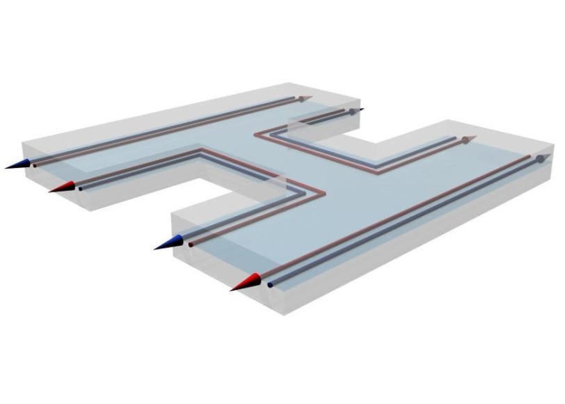
The potential advantage of using topological insulators to carry currents in chips is that electrons traveling along the thin surface of the material do so with great efficiency and generate very little heat. It’s not just the thinness of the surface that plays a role; it’s the fact that these electrons exhibit something called the "quantum spin Hall effect," one of the spooky realizations of quantum mechanics. Unlike electrons in conventional materials, each electron in a topological insulator travels in a direction perpendicular to its spin.
The net effect is that the electrons flow smoothly in the same direction with no resistance, calmly swerving around obstacles – such as accidental contaminants or defects in the material – rather than colliding and veering off in all directions. As Zhang explains it, it’s the difference between a Ferrari speeding through a crowded marketplace and the same car cruising down a highway.
The excitement surrounding topological insulators is not confined to their potential usefulness in electronic devices. They could also give scientists insight into a wide variety of exotic phenomena, including hypothetical particles called axions, which could help to explain dark matter, and magnetic monopoles.
It was Zhang who, in 2006, helped set off a mad dash to investigate topological insulators by predicting that an alloy of mercury and tellurium would behave as one. Within a year, a group in Germany made this compound and showed that it did indeed work, but only at very low temperatures. In 2009, Chen, Shen, Fisher and their colleagues proved that bismuth telluride – a cheaper, more abundant and easier-to-handle material – is a topological insulator at room temperature, and the field really took off.
The latest result is “a significant step,” Zhang said, in the worldwide effort by many groups of scientists to harness the properties of these novel materials.

(Image courtesy Shoucheng Zhang)