Understanding Magnetic Memory One Layer at a Time
“Smaller, faster, cheaper" is Silicon Valley's mantra for progress. But as critical components shrink to near atomic dimensions, it’s becoming much more difficult for their developers to understand exactly how they operate before committing to product design and manufacturing.
By Mike Ross
“Smaller, faster, cheaper" is Silicon Valley's mantra for progress. But as critical components shrink to near atomic dimensions, it’s becoming much more difficult for their developers to understand exactly how they operate before committing to product design and manufacturing.
With their ability to detect a wide range of phenomena precisely in space and time, synchrotron X-ray pulses are now being used to reveal the nanometer- and picosecond-scale behavior of potential electronic components. A SLAC-led team of scientists has made just such a contribution. They showed why the magnetic orientation in a multilayered structure being considered for use in future computer memories requires more energy to switch between states than had been predicted by theory.
“Previous studies have shown that these devices require more energy than expected,” said researcher David Bernstein of the Stanford Institute for Materials and Energy Science, a joint institute of SLAC and Stanford University. “Since we can make ultrafast movies using Synchrotron X-rays, now we know why they need more energy to switch.”
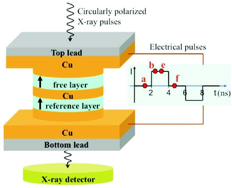
The experiments were conducted on a multilayered stack of metallic and magnetic materials similar to those being tested for use in magnetic random access memories, or MRAM. The magnetization direction of the top layer is perpendicular to the planes of the layers, an arrangement that enables smaller and more stable data bits and thus greater data-storage capacity and more-reliable operation. An “up” magnetic orientation stands for a “1” in the binary number system that computers use, and a “down” orientation represents a “0.” Shooting a short electrical pulse through the stack causes the top layer to change orientations.
Like today's flash memory, MRAM retains its information after a computer's power is turned off. But it is much faster and more durable than flash and could someday replace computers’ main memory, thus enabling instant-on high-performance computers. For MRAM to be commercially attractive, however, its physical size and power requirements must be reduced.
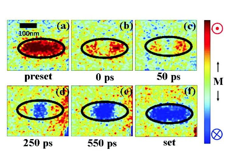
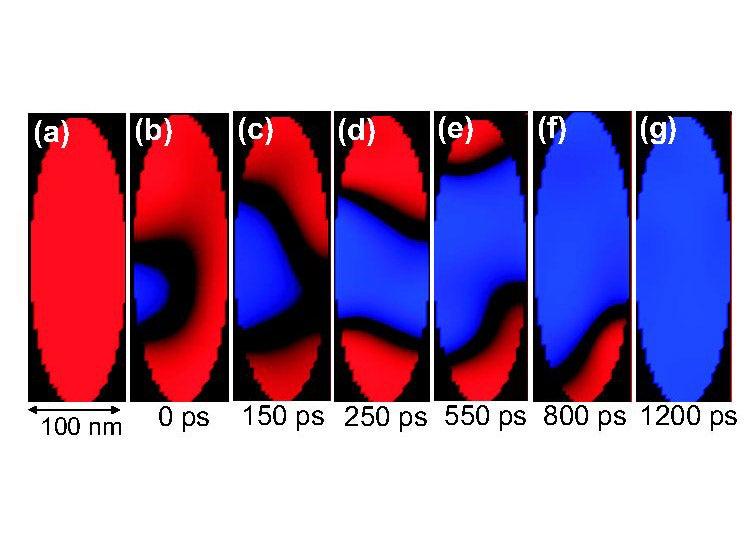
Instead of rotating from one orientation to the other all at once, the movies show the magnetic switching starting near the center of the pillar and spreading out toward the edges, creating two "domain wall" transition regions in the process. Although the walls move rapidly during the change – 100 meters a second through the tiny area less than 100,000th that of a human hair's cross section – their mere creation accounts for the extra energy use.
The scientists used a scanning soft-X-ray microscope at the Advanced Light Source synchrotron at Lawrence Berkeley National Laboratory to create and image millions of domain flips a second – billions in all. Varying the time interval between the electrical and X-ray pulses allowed the scientists to create ultrafast movies showing a detailed picoseconds-timescale account of exactly how the electrical pulse reversed the magnetic orientation.
The study was led by scientists from the Stanford Institute for Materials and Energy Research, or SIMES, and also included researchers from Lawrence Berkeley National Laboratory, Hitachi Global Technologies in San Jose, California; and technical institutes CNRS in Nancy, France, and ETH in Zurich, Switzerland. SIMES is a joint institute of SLAC National Accelerator Laboratory and Stanford University. The group's results were published in the May 10 edition of the technical journal Physics Review B.