A new way to watch atoms move in a single atomic sheet
X-ray laser snapshots give scientists a new tool for probing trillionths-of-a-second atomic motions in 2-D materials
Scientists have found a new way to use some of the world’s most powerful X-rays to watch how atoms move at ultrafast speeds within a single atomic sheet.
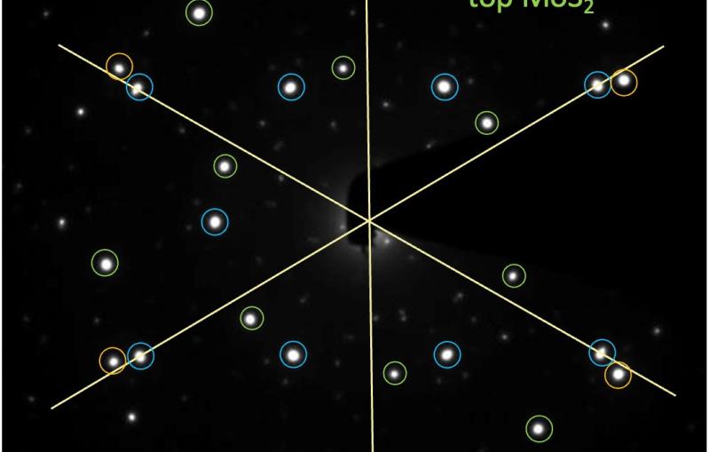
A study led by researchers at the U.S. Department of Energy’s Argonne National Laboratory, in collaboration with the University of Washington, DOE’s SLAC National Accelerator Laboratory and other institutions, developed the new technique, called ultrafast surface X-ray scattering. It revealed how the structure of an atomically thin, two-dimensional crystal changed after it was hit with an optical laser pulse.
Unlike previous X-ray scattering techniques, this new method goes beyond providing a static picture of the atoms on a material’s surface to capture the motion of atoms on timescales as short as trillionths of seconds after laser excitation.
“This gives us a new way to probe structural distortions in 2-D materials as they evolve, and to understand how they are related to unique properties of these materials that we hope to harness for electronic devices that use, emit or control light,” said Aaron Lindenberg, a professor at SLAC and Stanford University and collaborator on the study. “These approaches are also applicable to a broad class of other interesting and poorly understood phenomena that occur at the interfaces between materials.”
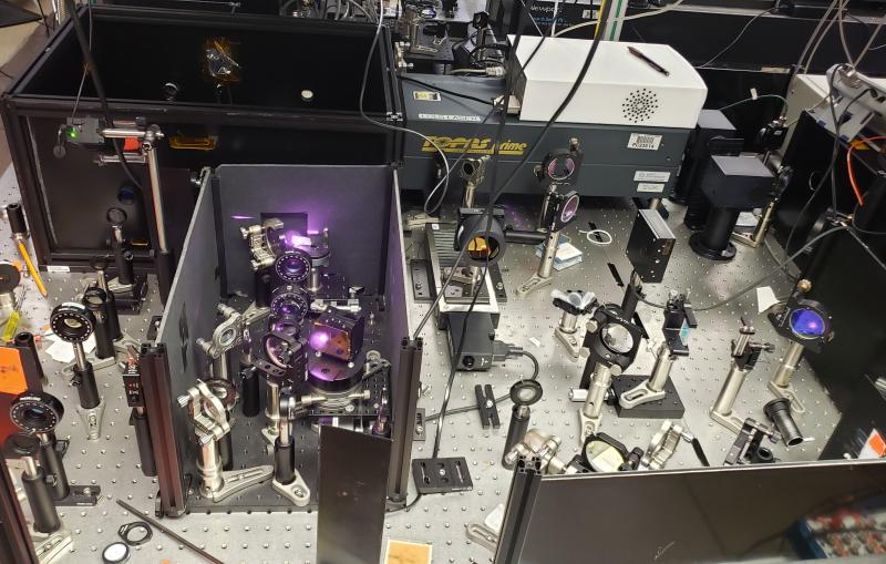
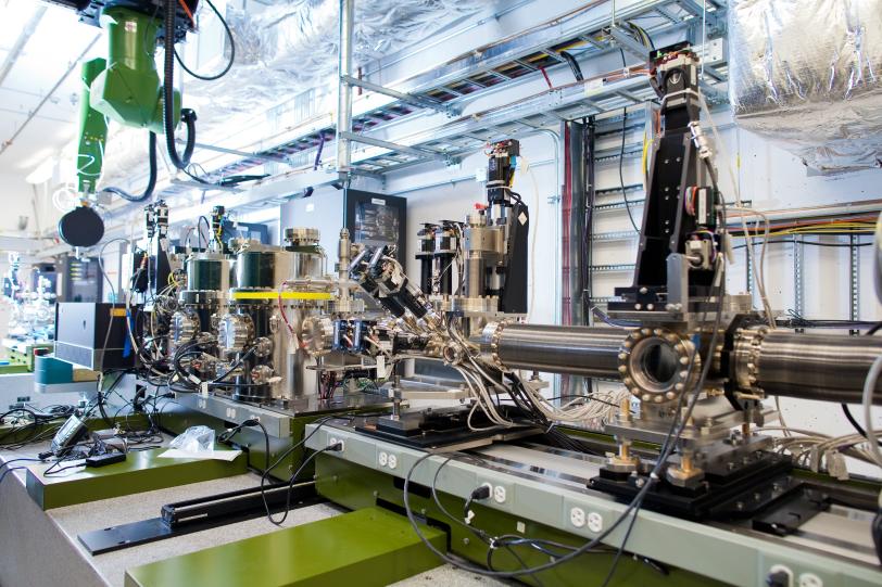
The experiments were carried out with the Linac Coherent Light Source (LCLS) X-ray free-electron laser at SLAC, which provides very bright X-rays in pulses just 50 femtoseconds – quadrillionths of a second – long. The team reported the results in the March 11 online edition of Nature Photonics.
“Surface X-ray scattering is challenging enough on its own,” said Argonne X-ray physicist and study co-author Hua Zhou. “Extending it to do ultrafast science in single-layer materials represents a major technological advance that can show us a great deal about how atoms behave at surfaces and at the interfaces between materials.”
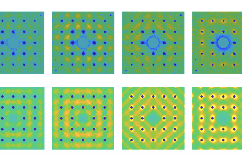
Argonne physicist Haidan Wen and postdoctoral researcher I-Cheng Tung led an investigation of a 2-D material called tungsten diselenide. In this material, each tungsten atom is connected to two selenium atoms in a “V” shape, forming a single layer that’s three atoms thick.
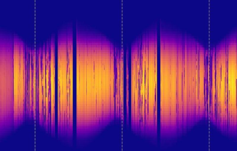
The atoms in 2-D materials typically vibrate slightly in all directions, Wen said. But when the team hit the material with optical laser pulses and watched what happened through ultrafast surface X-ray scattering, a different picture of atomic behavior emerged.
“You normally would expect the atoms to move out of the plane, since that’s where the available space is,” Wen said. “But here we see them mostly vibrate within the plane right after excitation.”
These observations were supported by first-principle calculations led by Aiichiro Nakano at University of Southern California and scientist Pierre Darancet of Argonne’s Center for Nanoscale Materials (CNM).
The direction of atomic shifts and other changes in the atomic lattice have important effects on the properties of 2-D materials like tungsten diselenide, according to University of Washington professor Xiaodong Xu.
“Because these 2-D materials have rich physical properties, scientists are interested in using them to explore fundamental phenomena, as well as potential applications in electronics and photonics,” he said. “Visualizing the motion of atoms in single atomic crystals is a true breakthrough and will allow us to understand and tailor material properties for energy relevant technologies.”
Preliminary surface X-ray scattering measurements were made at Argonne’s Advanced Photon Source (APS). Although those measurements were not taken at ultrafast speeds, they allowed the researchers to calibrate their approach for the LCLS free-electron laser experiments, Wen said.
The study also included researchers from Kumamoto University in Japan. APS, CNM and LCLS are DOE Office of Science User Facilities.
The research was funded by the DOE’s Office of Science.
This article is based on a press release from Argonne National Lab.
Citation: Tung et al., Nature Photonics, 11 March 2019 (10.1038/s41566-019-0387-5)
Contact
For questions or comments, contact the SLAC Office of Communications at communications@slac.stanford.edu.
SLAC is a multi-program laboratory exploring frontier questions in photon science, astrophysics, particle physics and accelerator research. Located in Menlo Park, Calif., SLAC is operated by Stanford University for the U.S. Department of Energy's Office of Science.
SLAC National Accelerator Laboratory is supported by the Office of Science of the U.S. Department of Energy. The Office of Science is the single largest supporter of basic research in the physical sciences in the United States, and is working to address some of the most pressing challenges of our time.
Related stories