Researchers Use World's Smallest Diamonds to Make Wires Three Atoms Wide
LEGO-style Building Method Has Potential for Making One-Dimensional Materials with Extraordinary Properties
Menlo Park, Calif. — Scientists at Stanford University and the Department of Energy’s SLAC National Accelerator Laboratory have discovered a way to use diamondoids – the smallest possible bits of diamond – to assemble atoms into the thinnest possible electrical wires, just three atoms wide.
By grabbing various types of atoms and putting them together LEGO-style, the new technique could potentially be used to build tiny wires for a wide range of applications, including fabrics that generate electricity, optoelectronic devices that employ both electricity and light, and superconducting materials that conduct electricity without any loss. The scientists reported their results today in Nature Materials.
“What we have shown here is that we can make tiny, conductive wires of the smallest possible size that essentially assemble themselves,” said Hao Yan, a Stanford postdoctoral researcher and lead author of the paper. “The process is a simple, one-pot synthesis. You dump the ingredients together and you can get results in half an hour. It’s almost as if the diamondoids know where they want to go.”
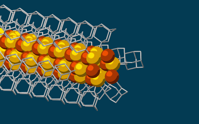
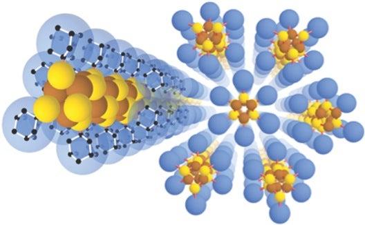
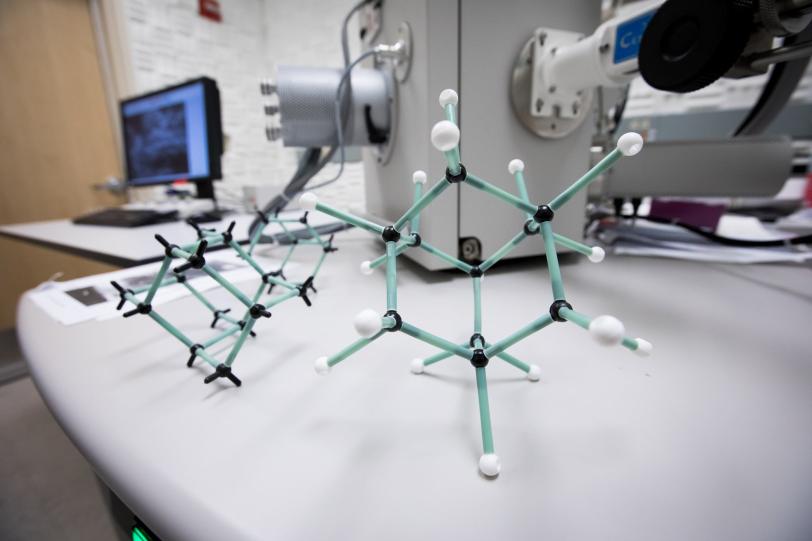
This animation shows molecular building blocks joining the tip of a growing nanowire. Each block consists of a diamondoid – the smallest possible bit of diamond – attached to sulfur and copper atoms (yellow and brown spheres). Like LEGO blocks, they only fit together in certain ways that are determined by their size and shape. The copper and sulfur atoms form a conductive wire in the middle, and the diamondoids form an insulating outer shell. (SLAC National Accelerator Laboratory)
The Smaller the Better
Although there are other ways to get materials to self-assemble, this is the first one shown to make a nanowire with a solid, crystalline core that has good electronic properties, said study co-author Nicholas Melosh, an associate professor at SLAC and Stanford and investigator with SIMES, the Stanford Institute for Materials and Energy Sciences at SLAC.
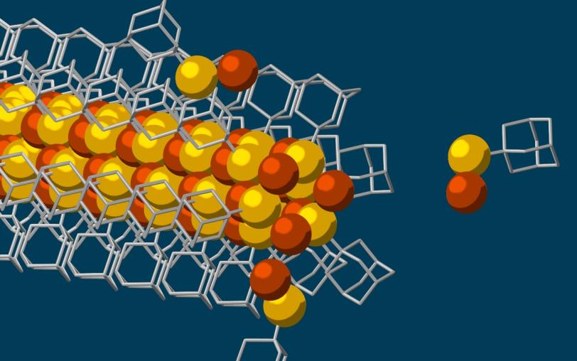
The needle-like wires have a semiconducting core – a combination of copper and sulfur known as a chalcogenide – surrounded by the attached diamondoids, which form an insulating shell.
Their minuscule size is important, Melosh said, because a material that exists in just one or two dimensions – as atomic-scale dots, wires or sheets – can have very different, extraordinary properties compared to the same material made in bulk. The new method allows researchers to assemble those materials with atom-by-atom precision and control.
The diamondoids they used as assembly tools are tiny, interlocking cages of carbon and hydrogen. Found naturally in petroleum fluids, they are extracted and separated by size and geometry in a SLAC laboratory. Over the past decade, a SIMES research program led by Melosh and SLAC/Stanford Professor Zhi-Xun Shen has found a number of potential uses for the little diamonds, including improving electron microscope images and making tiny electronic gadgets.
Constructive Attraction
For this study, the research team took advantage of the fact that diamondoids are strongly attracted to each other, through what are known as van der Waals forces. (This attraction is what makes the microscopic diamondoids clump together into sugar-like crystals, which is the only reason you can see them with the naked eye.)
They started with the smallest possible diamondoids – single cages that contain just 10 carbon atoms – and attached a sulfur atom to each. Floating in a solution, each sulfur atom bonded with a single copper ion. This created the basic nanowire building block.
The building blocks then drifted toward each other, drawn by the van der Waals attraction between the diamondoids, and attached to the growing tip of the nanowire.
“Much like LEGO blocks, they only fit together in certain ways that are determined by their size and shape,” said Stanford graduate student Fei Hua Li, who played a critical role in synthesizing the tiny wires and figuring out how they grew. “The copper and sulfur atoms of each building block wound up in the middle, forming the conductive core of the wire, and the bulkier diamondoids wound up on the outside, forming the insulating shell.”
A Versatile Toolkit for Creating Novel Materials
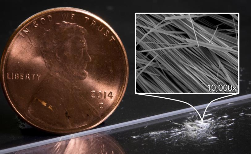
The team has already used diamondoids to make one-dimensional nanowires based on cadmium, zinc, iron and silver, including some that grew long enough to see without a microscope, and they have experimented with carrying out the reactions in different solvents and with other types of rigid, cage-like molecules, such as carboranes.
The cadmium-based wires are similar to materials used in optoelectronics, such as light-emitting diodes (LEDs), and the zinc-based ones are like those used in solar applications and in piezoelectric energy generators, which convert motion into electricity.
“You can imagine weaving those into fabrics to generate energy,” Melosh said. “This method gives us a versatile toolkit where we can tinker with a number of ingredients and experimental conditions to create new materials with finely tuned electronic properties and interesting physics.”
Theorists led by SIMES Director Thomas Devereaux modeled and predicted the electronic properties of the nanowires, which were examined with X-rays at SLAC’s Stanford Synchrotron Radiation Lightsource, a DOE Office of Science User Facility, to determine their structure and other characteristics.
The team also included researchers from the Stanford Department of Materials Science and Engineering, Lawrence Berkeley National Laboratory, the National Autonomous University of Mexico (UNAM) and Justus-Liebig University in Germany. Parts of the research were carried out at Berkeley Lab’s Advanced Light Source (ALS) and National Energy Research Scientific Computing Center (NERSC), both DOE Office of Science User Facilities. The work was funded by the DOE Office of Science and the German Research Foundation.
Citation: Yan et al., Nature Materials, 26 December 2016 (10.1038/nmat4823)
Press Office Contact: Andrew Gordon, agordon@slac.stanford.edu, (650) 926-2282
SLAC is a multi-program laboratory exploring frontier questions in photon science, astrophysics, particle physics and accelerator research. Located in Menlo Park, California, SLAC is operated by Stanford University for the U.S. Department of Energy Office of Science. To learn more, please visit www.slac.stanford.edu.
SLAC National Accelerator Laboratory is supported by the Office of Science of the U.S. Department of Energy. The Office of Science is the single largest supporter of basic research in the physical sciences in the United States, and is working to address some of the most pressing challenges of our time. For more information, please visit science.energy.gov.
Related stories