SLAC’s Ultrafast ‘Electron Camera’ Visualizes Ripples in 2-D Material
Using a new technology for ultrafast science, researchers have for the first time observed extremely rapid atomic motions in a three-atom-thick layer of a promising material that could be used in next-generation solar cells, electronics and catalysts.
Menlo Park, Calif. — New research led by scientists from the Department of Energy’s SLAC National Accelerator Laboratory and Stanford University shows how individual atoms move in trillionths of a second to form wrinkles on a three-atom-thick material. Revealed by a brand new “electron camera,” one of the world’s speediest, this unprecedented level of detail could guide researchers in the development of efficient solar cells, fast and flexible electronics and high-performance chemical catalysts.
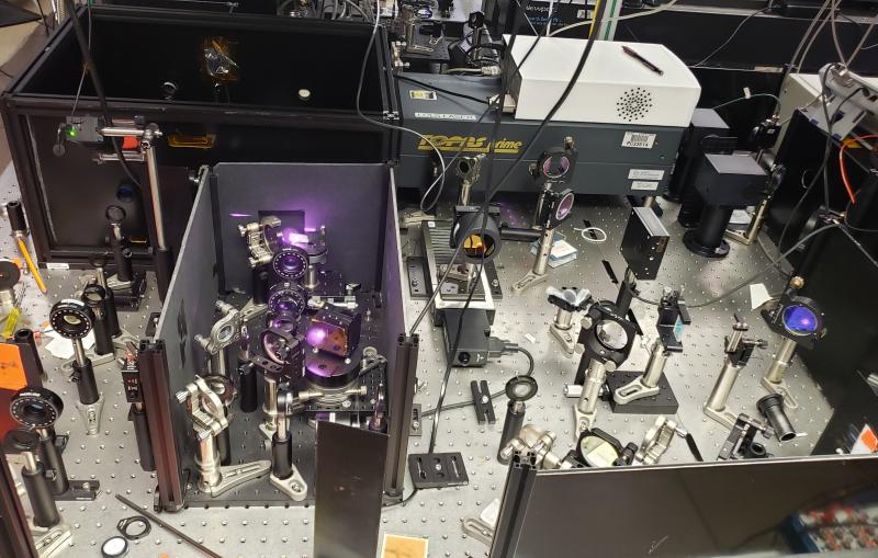
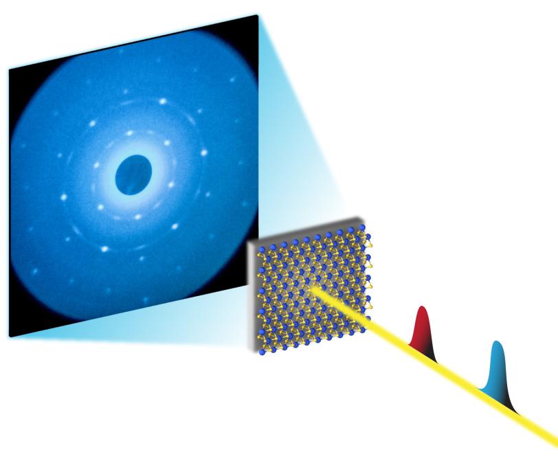
The breakthrough, accepted for publication Aug. 31 in Nano Letters, could take materials science to a whole new level. It was made possible with SLAC’s instrument for ultrafast electron diffraction (UED), which uses energetic electrons to take snapshots of atoms and molecules on timescales as fast as 100 quadrillionths of a second.
“This is the first published scientific result with our new instrument,” said scientist Xijie Wang, SLAC’s UED team lead. “It showcases the method’s outstanding combination of atomic resolution, speed and sensitivity.”
SLAC Director Chi-Chang Kao said, “Together with complementary data from SLAC’s X-ray laser Linac Coherent Light Source, UED creates unprecedented opportunities for ultrafast science in a broad range of disciplines, from materials science to chemistry to the biosciences.” LCLS is a DOE Office of Science User Facility.
Ultrafast Electron Diffraction: How It Works
This animation explains how researchers use high-energy electrons at SLAC to study faster-than-ever motions of atoms and molecules relevant to important material properties and chemical processes.
Greg Stewart/SLAC National Accelerator Laboratory
Extraordinary Material Properties in Two Dimensions
Monolayers, or 2-D materials, contain just a single layer of molecules. In this form they can take on new and exciting properties such as superior mechanical strength and an extraordinary ability to conduct electricity and heat. But how do these monolayers acquire their unique characteristics? Until now, researchers only had a limited view of the underlying mechanisms.
“The functionality of 2-D materials critically depends on how their atoms move,” said SLAC and Stanford researcher Aaron Lindenberg, who led the research team. “However, no one has ever been able to study these motions on the atomic level and in real time before. Our results are an important step toward engineering next-generation devices from single-layer materials.” The research team looked at molybdenum disulfide, or MoS2, which is widely used as a lubricant but takes on a number of interesting behaviors when in single-layer form – more than 150,000 times thinner than a human hair.
For example, the monolayer form is normally an insulator, but when stretched, it can become electrically conductive. This switching behavior could be used in thin, flexible electronics and to encode information in data storage devices. Thin films of MoS2 are also under study as possible catalysts that facilitate chemical reactions. In addition, they capture light very efficiently and could be used in future solar cells.
Because of this strong interaction with light, researchers also think they may be able to manipulate the material’s properties with light pulses.
“To engineer future devices, control them with light and create new properties through systematic modifications, we first need to understand the structural transformations of monolayers on the atomic level,” said Stanford researcher Ehren Mannebach, the study’s lead author.
Electron Camera Reveals Ultrafast Motions
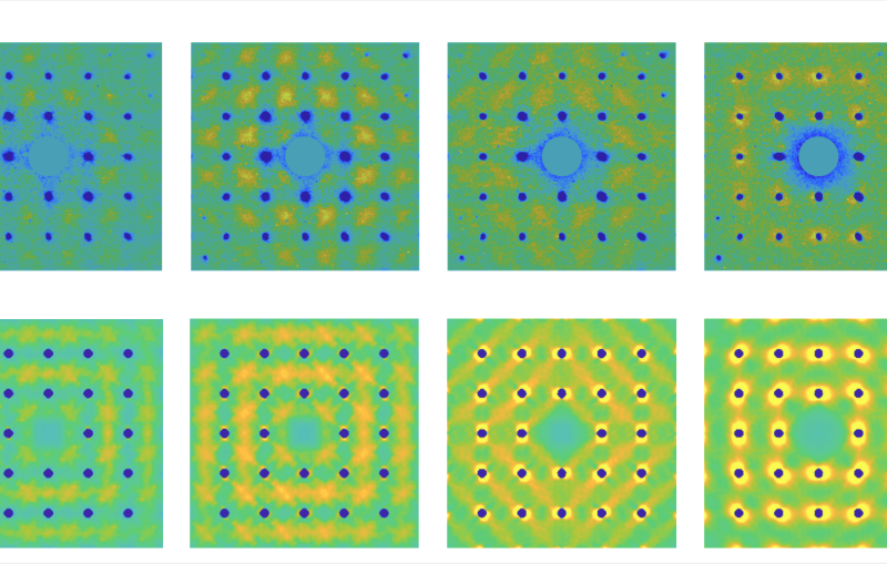
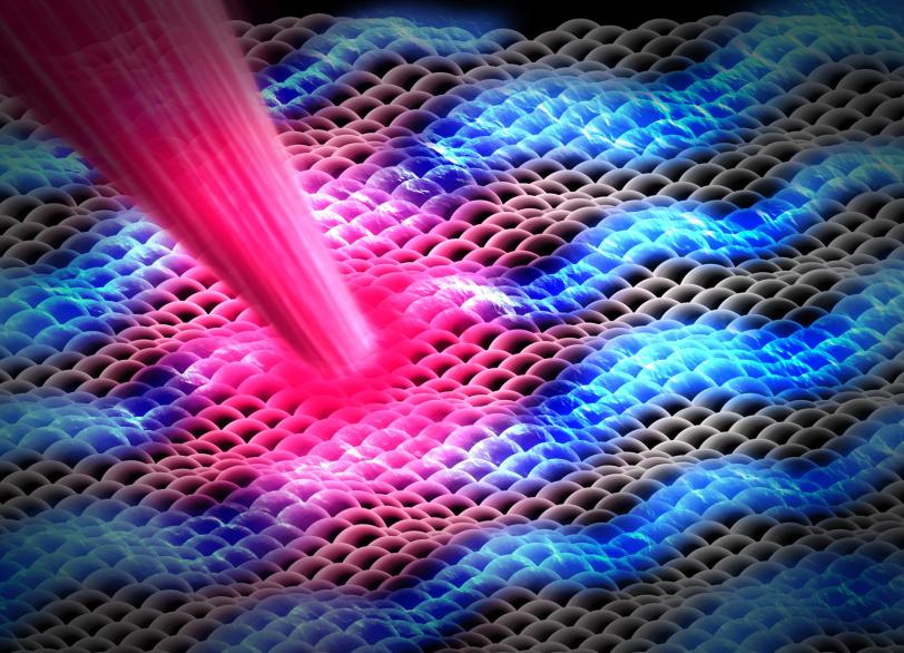
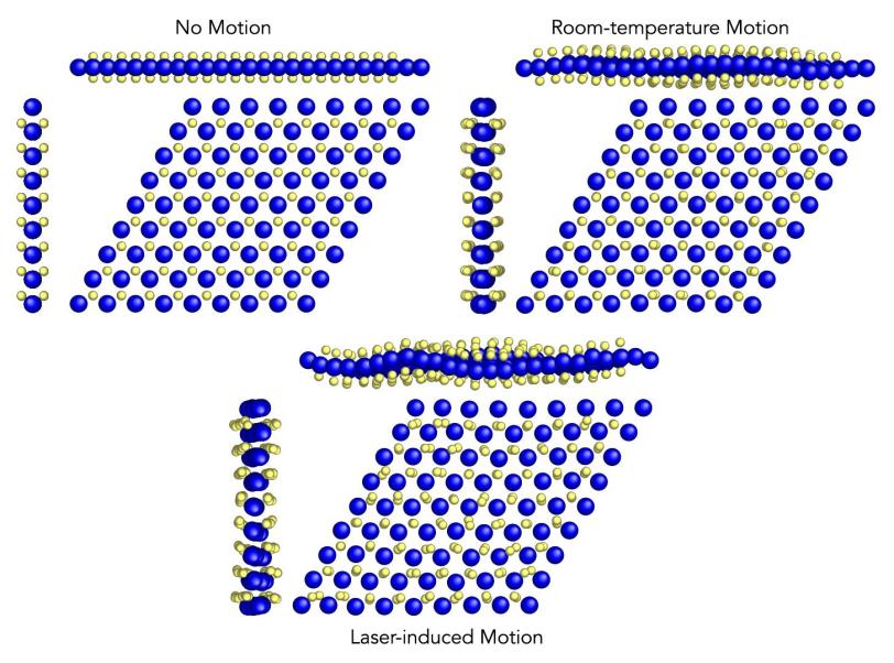
Previous analyses showed that single layers of molybdenum disulfide have a wrinkled surface. However, these studies only provided a static picture. The new study reveals for the first time how surface ripples form and evolve in response to laser light.
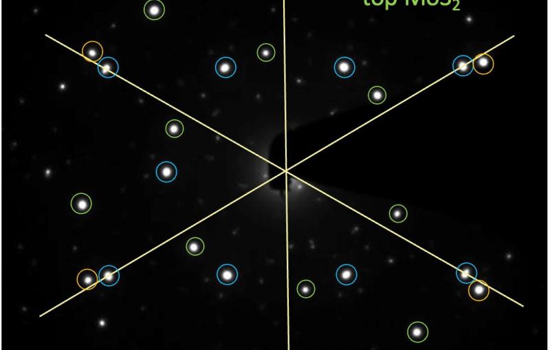
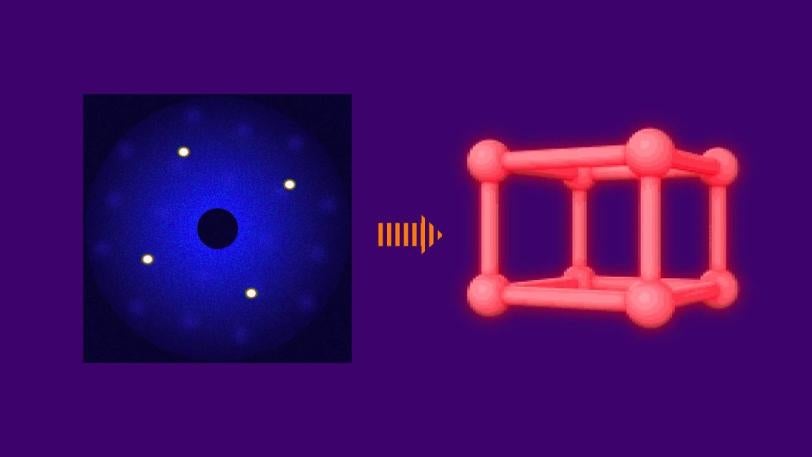
Researchers at SLAC placed their monolayer samples, which were prepared by Linyou Cao’s group at North Carolina State University, into a beam of very energetic electrons. The electrons, which come bundled in ultrashort pulses, scatter off the sample’s atoms and produce a signal on a detector that scientists use to determine where atoms are located in the monolayer. This technique is called ultrafast electron diffraction.
The team then used ultrashort laser pulses to excite motions in the material, which cause the scattering pattern to change over time.
“Combined with theoretical calculations, these data show how the light pulses generate wrinkles that have large amplitudes – more than 15 percent of the layer’s thickness – and develop extremely quickly, in about a trillionth of a second. This is the first time someone has visualized these ultrafast atomic motions,” Lindenberg said.
Once scientists better understand monolayers of different materials, they could begin putting them together and engineer mixed materials with completely new optical, mechanical, electronic and chemical properties.
The research was supported by DOE’s Office of Science, the SLAC UED/UEM program development fund, the German National Academy of Sciences, and the U.S. National Science Foundation.

Citation: E. M. Mannebach et al., Nano Letters, 31 August 2015 (10.1021/acs.nanolett.5b02805)
Press Office Contact: Manuel Gnida, mgnida@slac.stanford.edu, (650) 926-2632
SLAC is a vibrant multiprogram laboratory that explores how the universe works at the biggest, smallest and fastest scales and invents powerful tools used by scientists around the globe. With research spanning particle physics, astrophysics and cosmology, materials, chemistry, bio- and energy sciences and scientific computing, we help solve real-world problems and advance the interests of the nation.
SLAC is operated by Stanford University for the U.S. Department of Energy’s Office of Science. The Office of Science is the single largest supporter of basic research in the physical sciences in the United States and is working to address some of the most pressing challenges of our time.
Related stories