Microscopic Rake Doubles Efficiency of Low-cost Solar Cells
A SLAC/Stanford manufacturing technique could help make inexpensive polymer-based solar cells an attractive alternative to silicon-crystal wafers.
Researchers from the Department of Energy’s SLAC National Accelerator Laboratory and Stanford University have developed a manufacturing technique that could double the electricity output of inexpensive solar cells by using a microscopic rake when applying light-harvesting polymers.
When commercialized, this advance could help make polymer solar cells an economically attractive alternative to those made with much more expensive silicon-crystal wafers.
In experiments, solar cells made with the tiny rake double the efficiency of cells made without it and are 18 percent better than cells made using a microscopic straightedge blade.
The research was led by Zhenan Bao, a chemical engineering professor at Stanford and a member of the Stanford Institute for Materials and Energy Sciences (SIMES), which is run jointly by SLAC and Stanford. The team reported its results August 12 in Nature Communications.
“The fundamental scientific insights that come out of this work will give manufacturers a rational approach to improving their processes, rather than relying simply on trial and error,” Bao said.
“We also expect this simple, effective and versatile concept will be broadly applicable to making other polymer devices where properly aligning the molecules is important.”
The Problem With Polymers
Although prices for silicon-based solar cells are dropping, it still takes five to 15 years before they produce enough electricity to offset their purchase and installation. Silicon solar cells also require a large amount of energy to manufacture, which partly offsets their value as renewable energy sources.
Polymer-based photovoltaic cells are much cheaper because they’re made of inexpensive materials that can be simply painted or printed in place. They are also flexible and require little energy to manufacture. While small, lab-scale samples can convert more than 10 percent of sunlight into electricity, the large-area coated cells have very low efficiency – typically converting less than 5 percent, compared with 20-25 percent for commercial silicon-based cells.
Polymer cells typically combine two types of polymers: A donor, which converts sunlight into electrons, and an acceptor, which stores the electrons until they can be removed from the cell as usable electricity. But when this mixture is deposited on a cell’s conducting surface during manufacturing, the two types tend to separate as they dry into an irregular assortment of large clumps, making it more difficult for the cell to produce and harvest electrons.
The SLAC/Stanford researchers’ solution is a manufacturing technique called “fluid-enhanced crystal engineering,” or FLUENCE, which was originally developed to improve the electrical conduction of organic semiconductors.
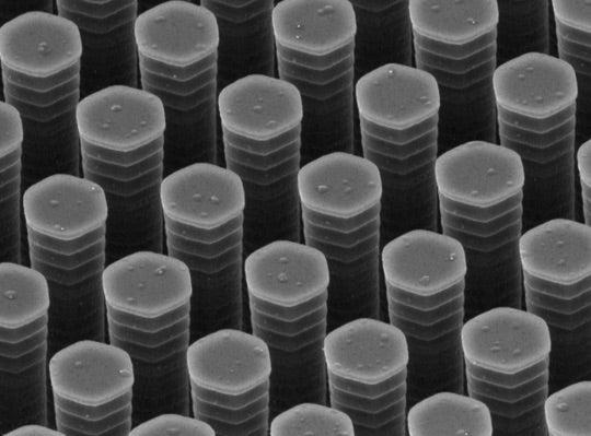
In the current work, as the polymers are painted onto a conducting surface, they are forced through a slightly angled rake containing several rows of stiff microscopic pillars. The rake is scraped along the surface at the relatively slow speed of 25-100 micrometers per second, which translates to 3.5-14.2 inches per hour. The large polymer molecules untangle and mix with each other as they bounce off and flow past the pillars, ultimately drying into tiny nanometer-sized crystals of uniform size with enhanced electrical properties.
Simulations and X-rays
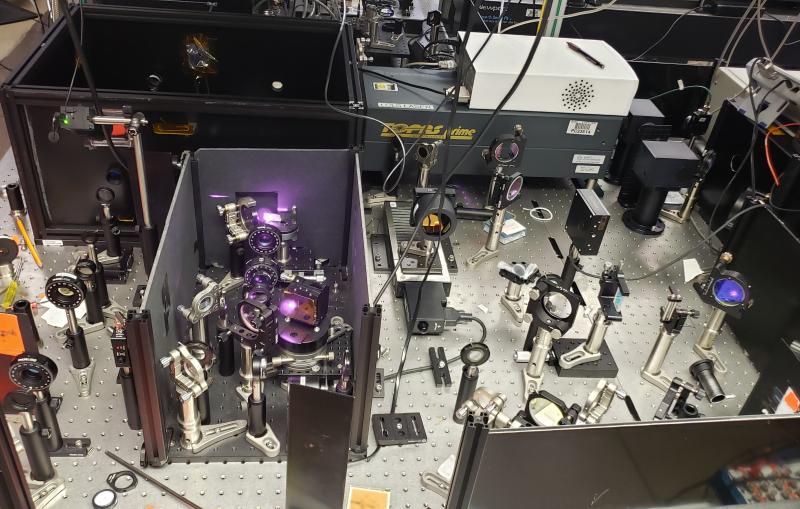
The researchers used computer simulations and X-ray analyses at two DOE Office of Science User Facilities -- SLAC’s Stanford Synchrotron Radiation Lightsource (SSRL) and Lawrence Berkeley National Laboratory’s Advanced Light Source (ALS) -- to customize the FLUENCE rake for making solar cells.
“At SSRL, the team used X-ray diffraction to measure the degree to which the polymers formed crystals and X-ray scattering to determine how clearly the two polymers segregated themselves,” said Mike Toney, SSRL Materials Sciences group leader and a co-author on the paper. “These are bread-and-butter techniques for which we’ve developed some novel approaches at SSRL in recent years.”
To achieve the polymer patterns they wanted for the solar cells, the researchers made the pillars in the rake much shorter and more densely packed than those used earlier for organic semiconductors. They were 1.5 micrometers high and 1.2 micrometers apart; for comparison, a human hair is about 100 micrometers in diameter.
Close, But Not Too Close
“Ideally, the two types of photovoltaic polymers should be close enough to each other for electrons to move quickly from donor to acceptor, but not so close that the acceptor gives back its electrons before they can be harvested to electricity,” said Yan Zhou, a Stanford researcher on Bao’s team.
“Our new FLUENCE rake achieves this happy medium. Because we understand what’s happening, we can tune the rake design and processing speed to alter the final polymer structures.”
Future research will be aimed at applying the FLUENCE technique to other polymer blends and adapting it to rapid industrial-scale roll-to-roll printing processes – which can reach speeds of 50 miles per hour – that promise the lowest solar-cell manufacturing costs.
The project began in October 2011 as a SLAC Laboratory Directed Research & Development project and is now funded by the Department of Energy’s Bridging Research Interactions through collaborative Development Grants in Energy (BRIDGE) program.
Collaborators in this research included former SLAC staff scientist Stefan Mannsfeld, who is now a professor at the Technical University in Dresden, Germany; former SIMES postdoctoral researcher Ying Diao, who is now a professor at the University of Illinois, and scientists from ALS, Peking University in China and Sungkyunkwan University in Korea.
Citation: Y. Diao, et al, Nature Communications, 12 August 2015 (10.1038/ncomms8955)
For questions or comments, contact the SLAC Office of Communications at communications@slac.stanford.edu.
SLAC is a multi-program laboratory exploring frontier questions in photon science, astrophysics, particle physics and accelerator research. Located in Menlo Park, Calif., SLAC is operated by Stanford University for the U.S. Department of Energy's Office of Science.
SLAC National Accelerator Laboratory is supported by the Office of Science of the U.S. Department of Energy. The Office of Science is the single largest supporter of basic research in the physical sciences in the United States, and is working to address some of the most pressing challenges of our time. For more information, please visit science.energy.gov.
(Z. Bao et al, Nature Communications)
Related stories