In a first, scientists watch 2D puddles of electrons spontaneously emerge in a 3D superconducting material
It’s an example of how surprising properties can spontaneously emerge in complex materials – a phenomenon scientists hope to harness for novel technologies.
By Glennda Chui
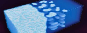
Creating a two-dimensional material, just a few atoms thick, is often an arduous process requiring sophisticated equipment. So scientists were surprised to see 2D puddles emerge inside a three-dimensional superconductor – a material that allows electrons to travel with 100% efficiency and zero resistance – with no prompting.
Within those puddles, superconducting electrons acted as if they were confined inside an incredibly thin, sheet-like plane, a situation that requires them to somehow cross over to another dimension, where different rules of quantum physics apply.
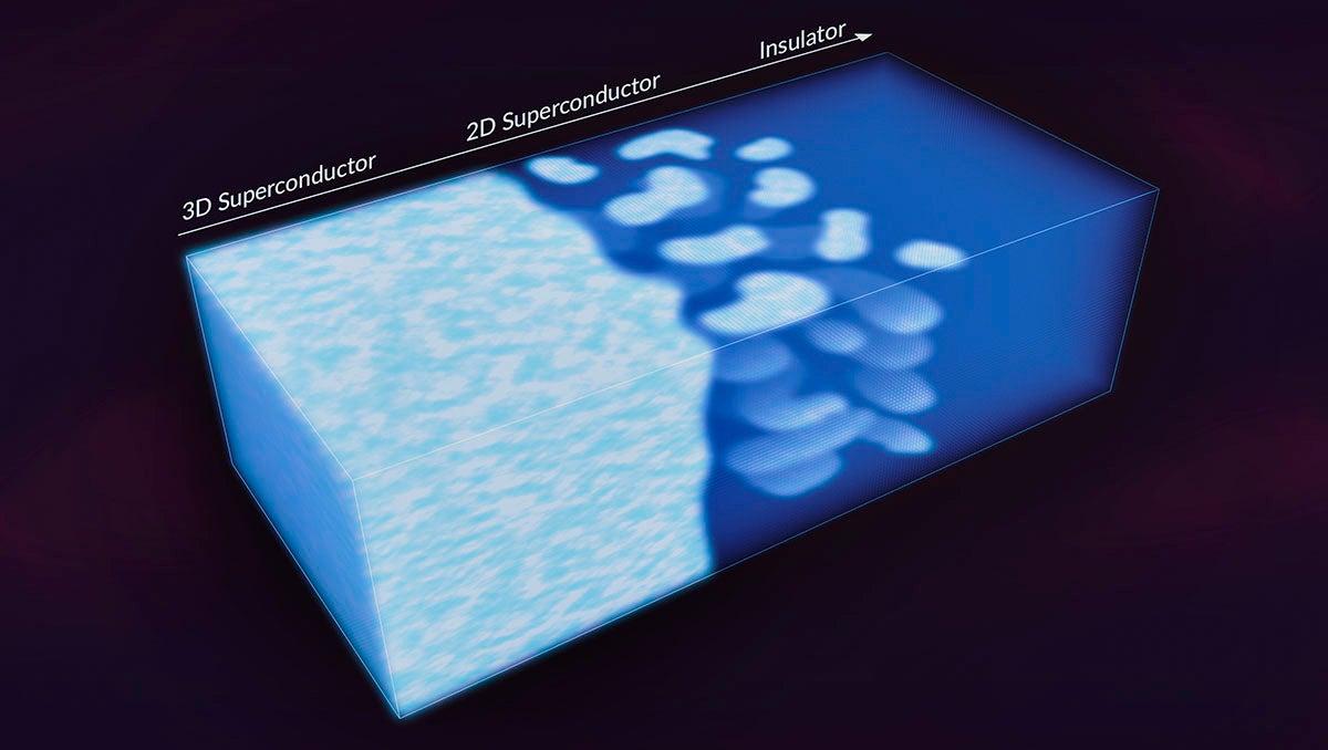
“This is a tantalizing example of emergent behavior, which is often difficult or impossible to replicate by trying to engineer it from scratch,” said Hari Manoharan, a professor at Stanford University and investigator with the Stanford Institute for Materials and Energy Sciences (SIMES) at the Department of Energy’s SLAC National Accelerator Laboratory, who led the research.
“It's as if when given the power to superconduct,” he said, “the 3D electrons choose for themselves to live in a 2D world.”
The research team calls this new phenomenon "inter-dimensional superconductivity," and in a report in the Proceedings of the National Academy of Sciences today, they suggest that this is how 3D superconductors reorganize themselves just before undergoing an abrupt shift into an insulating state, where electrons are confined to their home atoms and can’t move around at all.
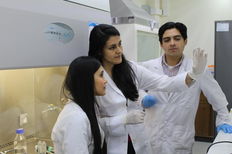
“What we found was a system where electrons behave in unexpected ways. That’s the beauty of physics,” said Carolina Parra, a postdoctoral researcher at SLAC and Stanford at the time of the study who carried out the experiments that led to the visualization of this intriguing result. “We were very lucky to find this behavior.”
Electrons acting strangely
Although superconductivity was discovered more than a century ago, its usefulness was limited by the fact that materials became superconducting only at temperatures close to those of deep space.
So the announcement in 1986 that scientists had discovered a new and unexpected class of superconducting materials that operated at much higher – although still very cold – temperatures set off a tsunami of research that continues to this day, with the goal of figuring out how the new materials operate and developing versions that work at closer to room temperature for applications such as perfectly efficient power lines and maglev trains.
This study started with a high-temperature superconductor named BPBO for its four atomic ingredients – barium, lead, bismuth and oxygen. It was synthesized in the lab of Stanford Professor and SIMES investigator Ian Fisher by Paula Giraldo-Gallo, a PhD student at the time.
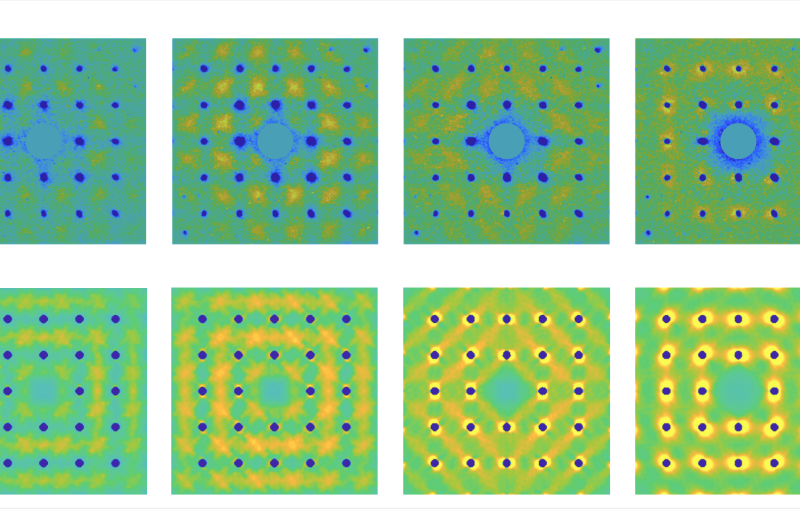
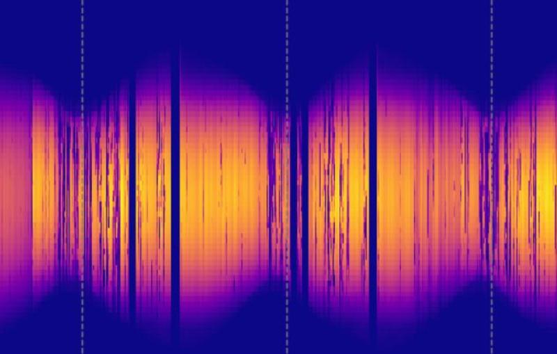
As researchers there put it through routine tests, including determining the transition temperature at which it flips between a superconducting and an insulating phase – like water changing to steam or ice – they realized that their data showed electrons behaving as if they were confined to ultrathin, 2D layers or stripes within the material. This was a puzzle, because BPBO is a 3D superconductor whose electrons are normally free to move in any direction they like.
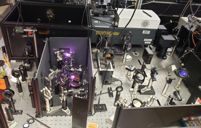
Intrigued, Manoharan’s team took a closer look with a scanning tunneling microscope, or STM – an instrument that can identify and even move individual atoms in the top few atomic layers of a material.
Interacting puddles
The stripes, they discovered, seemed to have no relationship with the way the material’s atoms were organized or with tiny bumps and dips on its surface.
“Instead, the stripes were layers where electrons behave as if they are confined to 2D, puddle-like areas in the material,” Parra said. “The distance between puddles is short enough that the electrons can ‘see’ and interact with each other in a way that allows them to move without resistance, which is the hallmark of superconductivity.”
The 2D puddles emerged as the scientists carefully adjusted the temperature and other conditions toward the transition point where the superconductor would become an insulator.
Their observations closely match a theory of “emergent electronic granularity” in superconductors, developed by Nandini Trivedi of Ohio State University and colleagues.
“The predictions we had made went against the standard paradigm for superconductors,” Trivedi said. “Usually, the stronger a superconductor is, the more the energy needed to break the bond between its superconducting electron pairs – a factor we call the energy gap. But my group had predicted that in this particular type of disordered superconductor, the opposite would be true: The system would form emergent puddles where superconductivity was strong but the pairs could be broken with much less energy than expected.
“It was quite thrilling to see those predictions being confirmed by the STM measurements from the Stanford group!”
Spreading the science
The results have practical implications for crafting 2D materials, Parra said.
“Most of the methods for making 2D materials are engineering approaches, like growing films a few atomic layers thick or creating a sharp interface between two materials and confining a 2D state there,” she said. “This offers an additional way to get to these 2D superconducting states. It’s cheaper, you don’t need fancy equipment that requires very low temperatures and it doesn’t take days and weeks. The only tricky part would be getting the composition of the material just right.”
Parra now heads a lab at the Federico Santa María Technical University in Valparaíso, Chile, focusing on interdisciplinary studies of nanoscale biological materials. She recently won a grant to acquire and operate the first-ever low-temperature scanning tunneling microscope in South America, which she plans to use to continue this line of research.
“When I have this equipment in the lab,” she said, “I will connect it with all the things I learned in Hari’s lab and use it to teach a new generation of researchers that we’re going to have working in nanoscience and nanotechnology in Chile.”
The research was funded by the DOE Office of Science.
Citation: Carolina Parra et al., Proceedings of the National Academy of Sciences, 12 April 2021 (10.1073/pnas.201781011)
For questions or comments, contact the SLAC Office of Communications at communications@slac.stanford.edu.
SLAC is a vibrant multiprogram laboratory that explores how the universe works at the biggest, smallest and fastest scales and invents powerful tools used by scientists around the globe. With research spanning particle physics, astrophysics and cosmology, materials, chemistry, bio- and energy sciences and scientific computing, we help solve real-world problems and advance the interests of the nation.
SLAC is operated by Stanford University for the U.S. Department of Energy’s Office of Science. The Office of Science is the single largest supporter of basic research in the physical sciences in the United States and is working to address some of the most pressing challenges of our time.
Related stories